Structure for a thin film multilayer capacitor

a multi-layer capacitor and structure technology, applied in the direction of fixed capacitors, fixed capacitor details, stacked capacitors, etc., can solve the problems of void filling, undulations often create fatal shorts in the overlying thin film region, and the void filling method cannot be used

Inactive Publication Date: 2000-02-08
IBM CORP
View PDF11 Cites 80 Cited by
  • Summary
  • Abstract
  • Description
  • Claims
  • Application Information

AI Technical Summary

Benefits of technology

FIG. 3 is a cross-sectional view of the layered substrate of FIG. 2 with a patterned

Problems solved by technology

In building a thin film capacitor structure on a ceramic interposer, the ceramic surface defects such as voids, pits, and undulations often create fatal shorts in the overlying thin film regions.
Further, conventional void filling approaches such as polymer fill cannot be used because the subsequent high temperature anneal required for dielectric film optimization is

Method used


Image

  • Structure for a thin film multilayer capacitor
  • Structure for a thin film multilayer capacitor
  • Structure for a thin film multilayer capacitor

Examples


Embodiment Construction

)

In describing the preferred embodiment of the present invention, reference will be made herein to FIGS. 1-10 of the drawings in which like numerals refer to like features of the invention. Features of the invention are not necessarily shown to scale in the drawings.

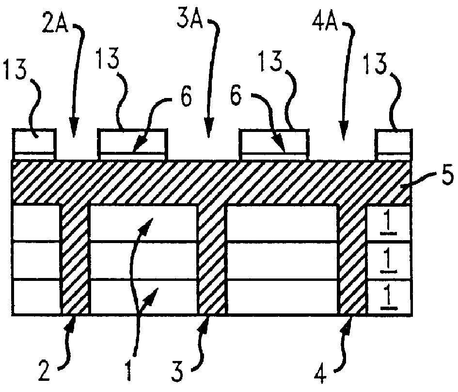
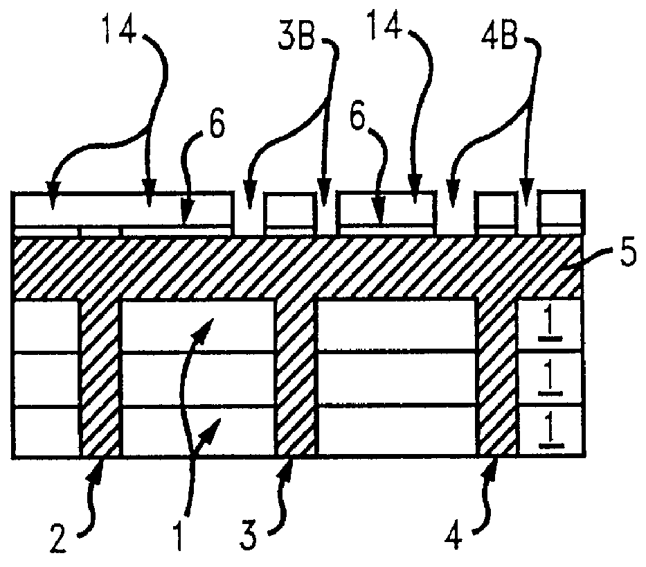
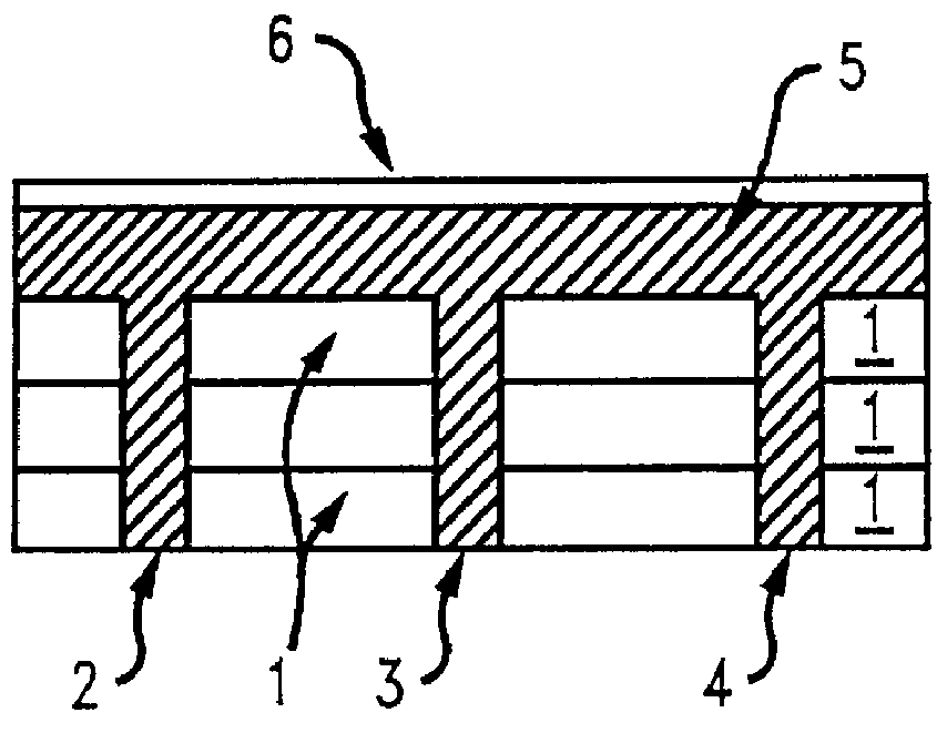
An interposer thin film capacitor structure is proposed, where the capacitor resides on a substrate, preferably a ceramic substrate. The complications associated with building this structure are derived chiefly from the pitted, rough surface of the ceramic substrate. The ceramic substrate is advantageous for processing at higher temperatures. However, the process yield is jeopardized by excessive fatal shorts on the overlying thin film region initiated by the pitted ceramic surface. The process described herein alleviates this deficiency, resulting in a ceramic thin film capacitor resilient to thin film shorting.

Referring initially to FIG. 1, a multilayer ceramic structure 20 is shown, comprised of at least one ceramic s...


PUM

PropertyMeasurementUnit
Currentaaaaaaaaaa
Thicknessaaaaaaaaaa
Dielectric polarization enthalpyaaaaaaaaaa

Abstract

An electronic component structure is proposed, wherein an interposer thin film capacitor structure is employed between an active electronic component and a multilayer circuit card. A method for making the interposer thin film capacitor is also proposed. In order to eliminate fatal electrical shorts in the overlying thin film regions that arise from pits, voids, or undulations on the substrate surface, a thick first metal layer, on the order of 0.5-10 mu m thick, is deposited on the substrate upon which the remaining thin films, including a dielectric film and second metal layer, are then applied. The first metal layer includes of Pt or other electrode metal, or a combination of Pt, Cr, and Cu metals, and a diffusion barrier layer. Additional Ti layers may be employed for adhesion enhancement. The thickness of the first metal layers are approximately: 200 A for the Cr layer; 0.5-10 mu m for the Cu layer; 1000 A-5000 A for the diffusion barrier; and 100 A-2500 A for a Pt layer.

Description

1. Field of the InventionThe present invention relates to multilayer electronic components and, in particular, to thin film multilayer capacitors and a method for making the same.2. Description of Related ArtMultilayer substrates with capacitors have found widespread use in electronics as integrated circuit packages. Multilayer capacitors consist of a plurality of interleaved and staggered layers of an electrically conductive film of metal and electrically insulating layers of a ceramic oxide (dielectric). Such capacitors are well known in the art. For example, U.S. Pat. No. 2,389,420 issued to A. J. Deyrup on Nov. 20, 1945, entitled, "MANUFACTURE OF CAPACITORS", describes the structure, manufacture, and properties of monolithic multilayer ceramic capacitors.Typically, multilayer ceramic capacitors are manufactured by building up an interleaved configuration of metal electrodes and ceramic layers, dicing individual parts out of the build-up, then subjecting the parts to a slow burno...

Claims


Application Information

Patent Timeline
IPC IPC(8): H01L21/02H01G4/30H01L27/04H01G4/33H01L21/822
CPCH01G4/306H01L28/40Y10T29/435
Inventor FAROOQ, MUKTA S.FAROOQ, SHAJIHAMEL, HARVEY C.KNICKERBOCKER, JOHN U.RITA, ROBERT A.STOLLER, HERBERT I.
Owner IBM CORP
Why Eureka
Try Eureka