Electrostatic protection circuit in a semiconductor device

a protection circuit and electrostatic technology, applied in the direction of overvoltage protection resistors, emergency protection arrangements for limiting excess voltage/current, and arrangements responsive to excess voltage, etc., can solve the problems of increasing data pin capacitance, data pin capacitance, and data pin capacitan

Inactive Publication Date: 2000-02-29
HYUNDAI ELECTRONICS IND CO LTD
View PDF5 Cites 13 Cited by
  • Summary
  • Abstract
  • Description
  • Claims
  • Application Information

AI Technical Summary

Problems solved by technology

Therefore, problems related to data pin capacitance and an electrostatic protection circuit have been raised.
Such an electrostatic protection circuit brings about the problem of increasing the data pin capacitance.
Distance A between gate b and contact c is too long for protecting the static electricity, and area B of an operation region being connected to a pad is also too long, thereby increasing the data pin capacitance due to increment of junction capacitance.
However, it is difficult to decrease the distance between a gate electrode and a contact in circuit structure of FIGS. 1, 2 and 10.

Method used


Image

  • Electrostatic protection circuit in a semiconductor device
  • Electrostatic protection circuit in a semiconductor device
  • Electrostatic protection circuit in a semiconductor device

Examples


Embodiment Construction

Below, embodiments of the present invention will be explained with reference to attached drawings.

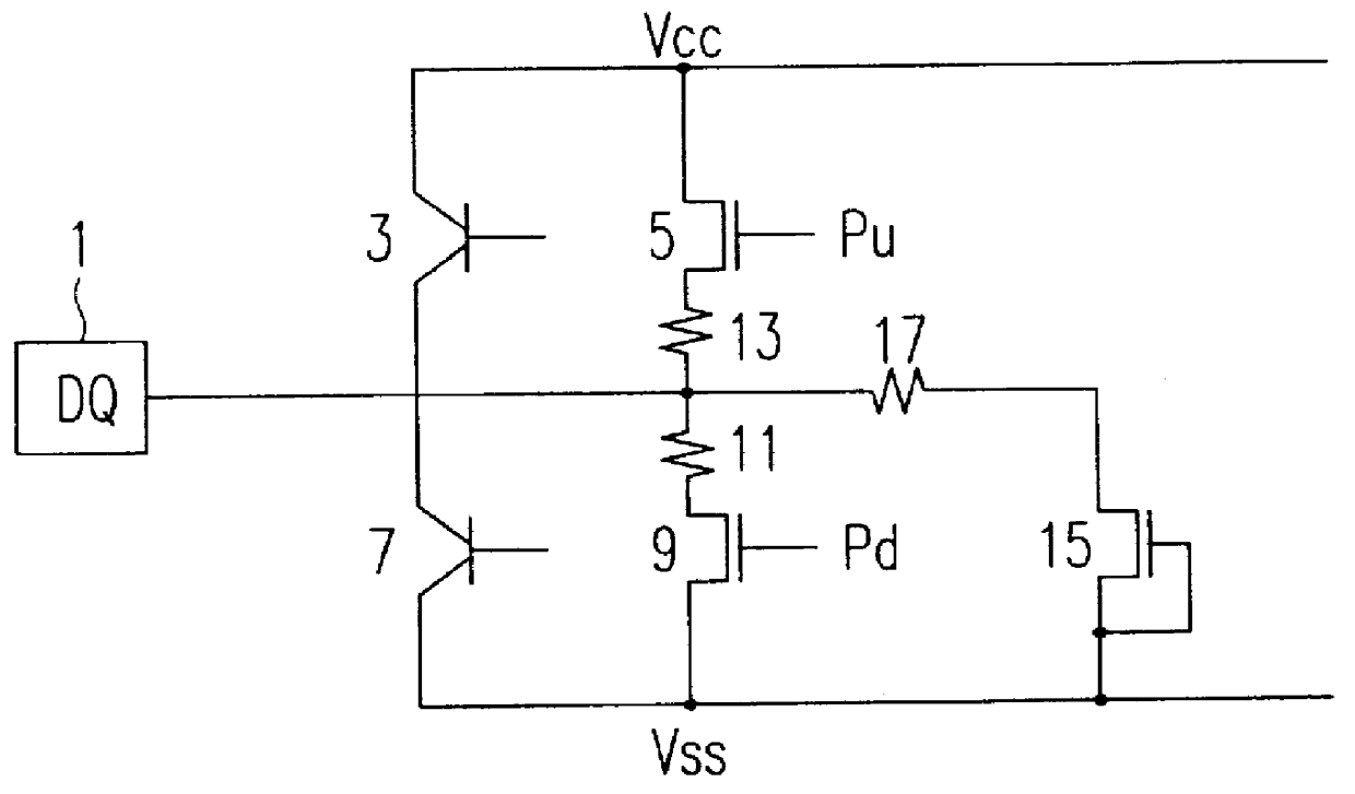
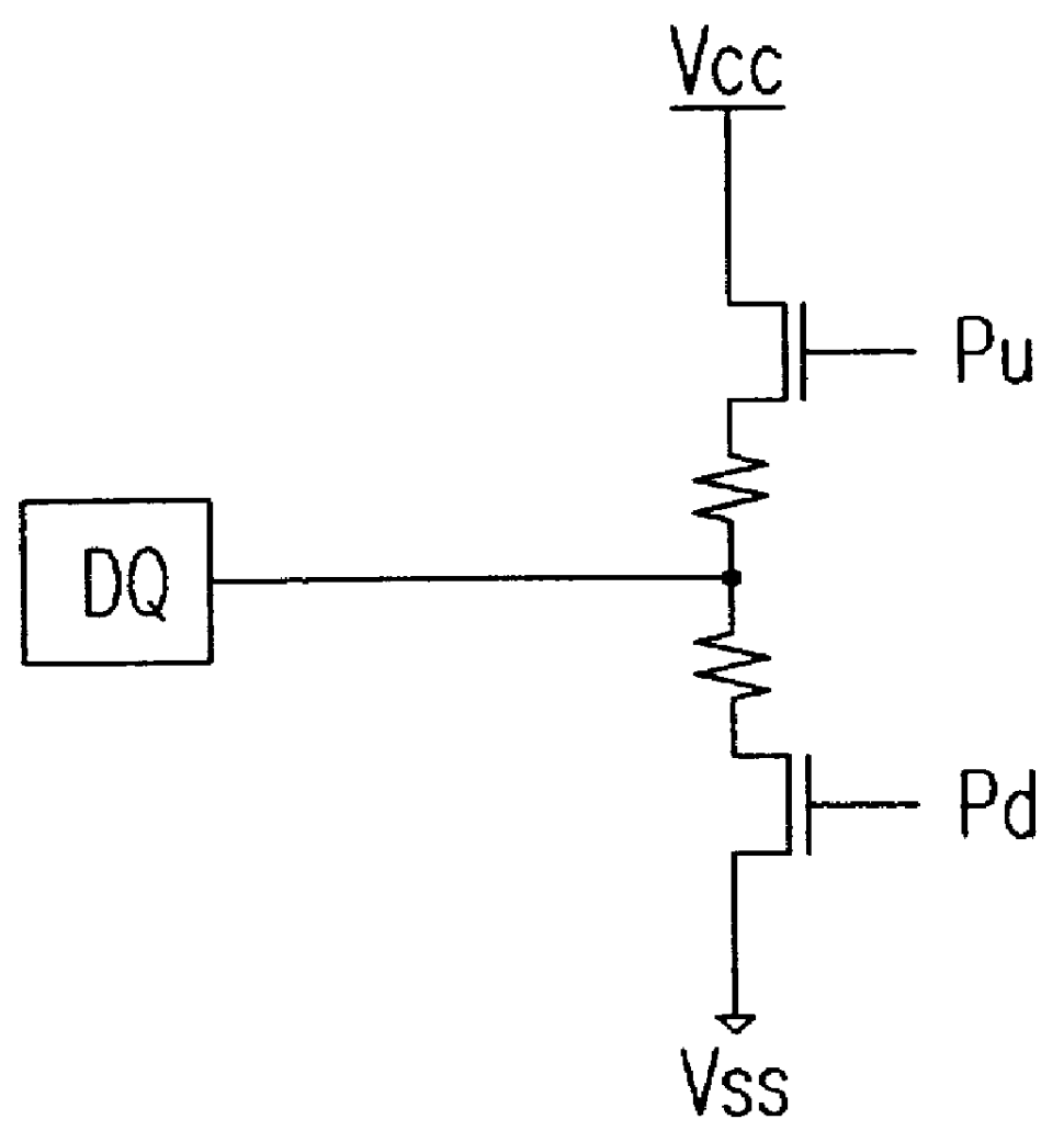
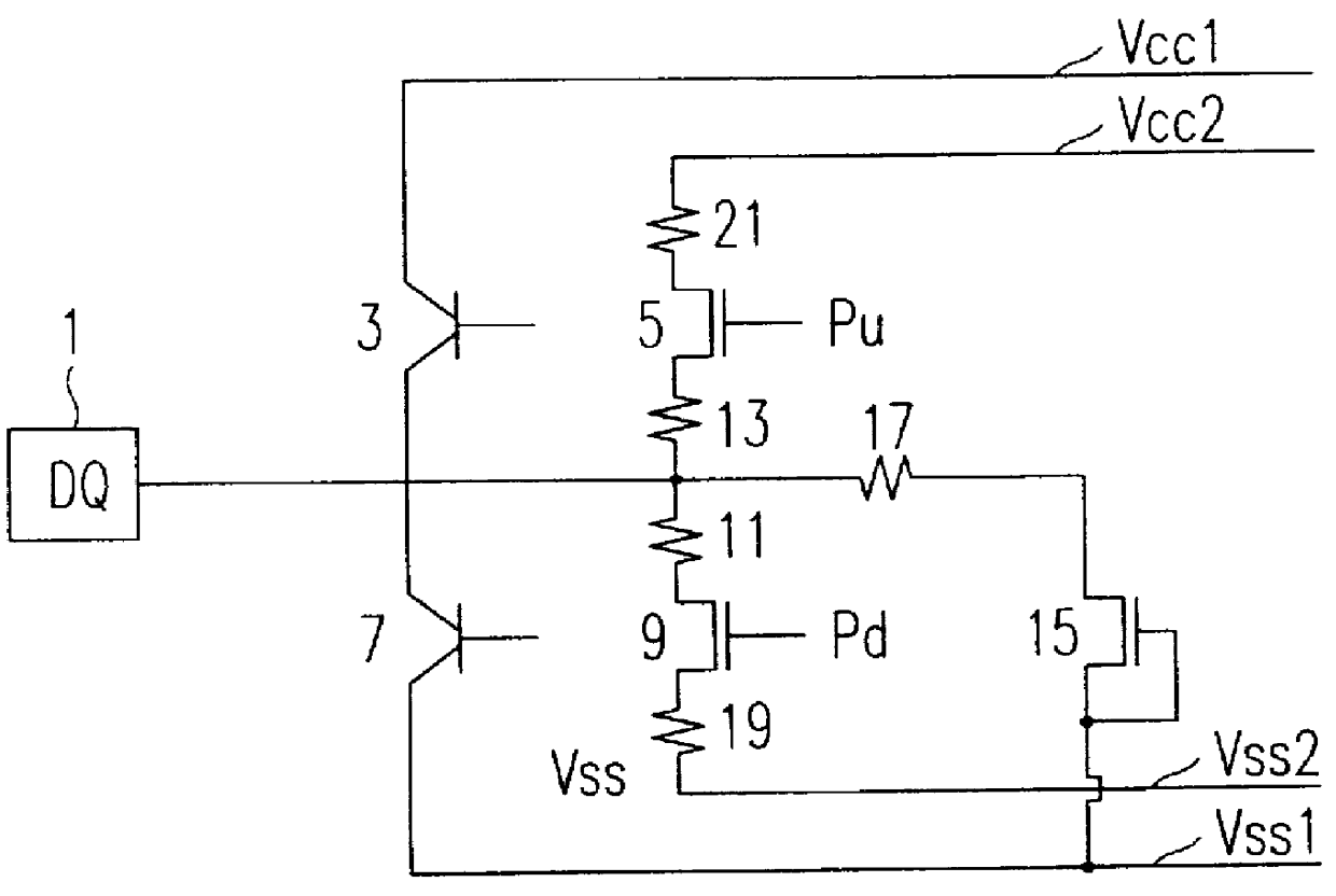
FIG. 3 is an electrostatic protection circuit of a data input and output pad 1 according to the present invention. A second bipolar transistor 3 is coupled between the pad 1 and a power line Vcc and an second active transistor 5 which is a pull up transistor is also coupled between the pad 1 and the power line Vcc. A first bipolar transistor 7 is coupled between the pad 1 and a ground line Vss and a first active transistor 9 which is a pull up transistor is also coupled between the pad 1 and the power line Vss. A fourth resistor 13 is coupled between the pad 1 and the second active transistor 5, and a first resistor 11 is coupled between the pad 1 and the first active transistor 9.

A third resistor 17 and an active diode transistor 15 are in series coupled between the pad 1 and the ground line Vss. A fifth resistor 21 is coupled between the pad 1 and the second active transistor 5. A sec...


PUM


Abstract

A power line and a ground line of a bipolar transistor for the electrostatic protection are isolated from a power line and a ground line of an active transistor for data input and output. Also, a resistor is coupled between a power line and a ground line of an active transistor for data input and output, and another resistor is coupled between a pad and the active transistor. Accordingly, the active transistor for data input and output is operated as an internal circuit in the electrostatic protection test since main current flows toward the bipolar transistor. An electrostatic protection circuit according to the present invention uses a bipolar transistor for the electrostatic protection and uses an active transistor for data input and output as an internal circuit in order to increase transistor size. Accordingly, a rated current of a data input and output pad is satisfied as well as the data pin capacitance is reduced since the distance between a gate and a contact in an active transistor is decreased.

Description

This invention relates to an electrostatic protection circuit. In particular, it relates to an electrostatic protection circuit that can satisfy a rated current of a data input and output pad and have small capacitance.DESCRIPTION OF THE RELATED PRIOR ARTRecently, a semiconductor has been highly integrated and various semiconductor products have been developed. Therefore, problems related to data pin capacitance and an electrostatic protection circuit have been raised. Conventional electrostatic protection circuits as shown in FIGS. 1 and 2 will be explained with reference to a layout of FIG. 10.FIG. 1 shows a conventional electrostatic protection circuit in a data input and output pad. A bipolar transistor for electrostatic protection is coupled between a Vcc power line and a pad, and between a Vss ground line and the pad. A pull up transistor is coupled to the Vcc power line, and a pull down transistor is coupled to the Vss ground line.In FIG. 1, during an electrostatic test, the ...

Claims


Application Information

Patent Timeline
Patent Type & Authority Patents(United States)
IPC IPC(8): H01L27/02H01L27/04
CPCH01L27/0251H01L27/0259H01L27/0266H01L27/04
Inventor JEONG, JAE GOAN
Owner HYUNDAI ELECTRONICS IND CO LTD
Why Eureka
Try Eureka