
Silicon on insulator domino logic circuits

a logic circuit and silicon technology, applied in logic circuits, pulse techniques, electric pulse generator details, etc., can solve the problem of charge sharing in the circuit of cmos domino logic circuits

Inactive Publication Date: 2000-04-11
IBM CORP
View PDF3 Cites 10 Cited by
  • Summary
  • Abstract
  • Description
  • Claims
  • Application Information

AI Technical Summary

Problems solved by technology

Although CMOS technology offers various advantages, such as low power consumption and stability, over other types of processing technologies, one major drawback of CMOS domino logic circuits is the effect of charge sharing.

Method used


Image

  • Silicon on insulator domino logic circuits
  • Silicon on insulator domino logic circuits
  • Silicon on insulator domino logic circuits

Examples


Embodiment Construction

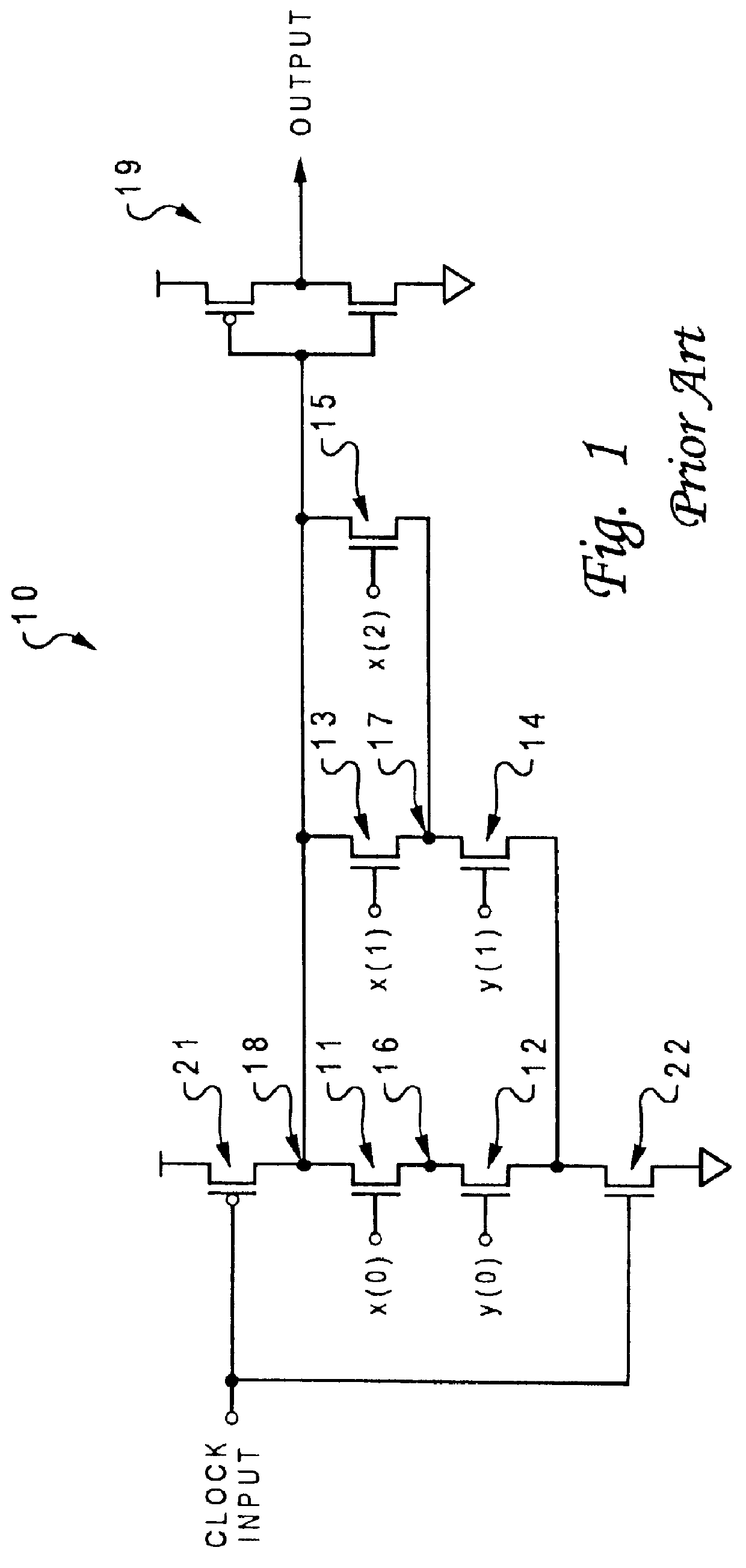
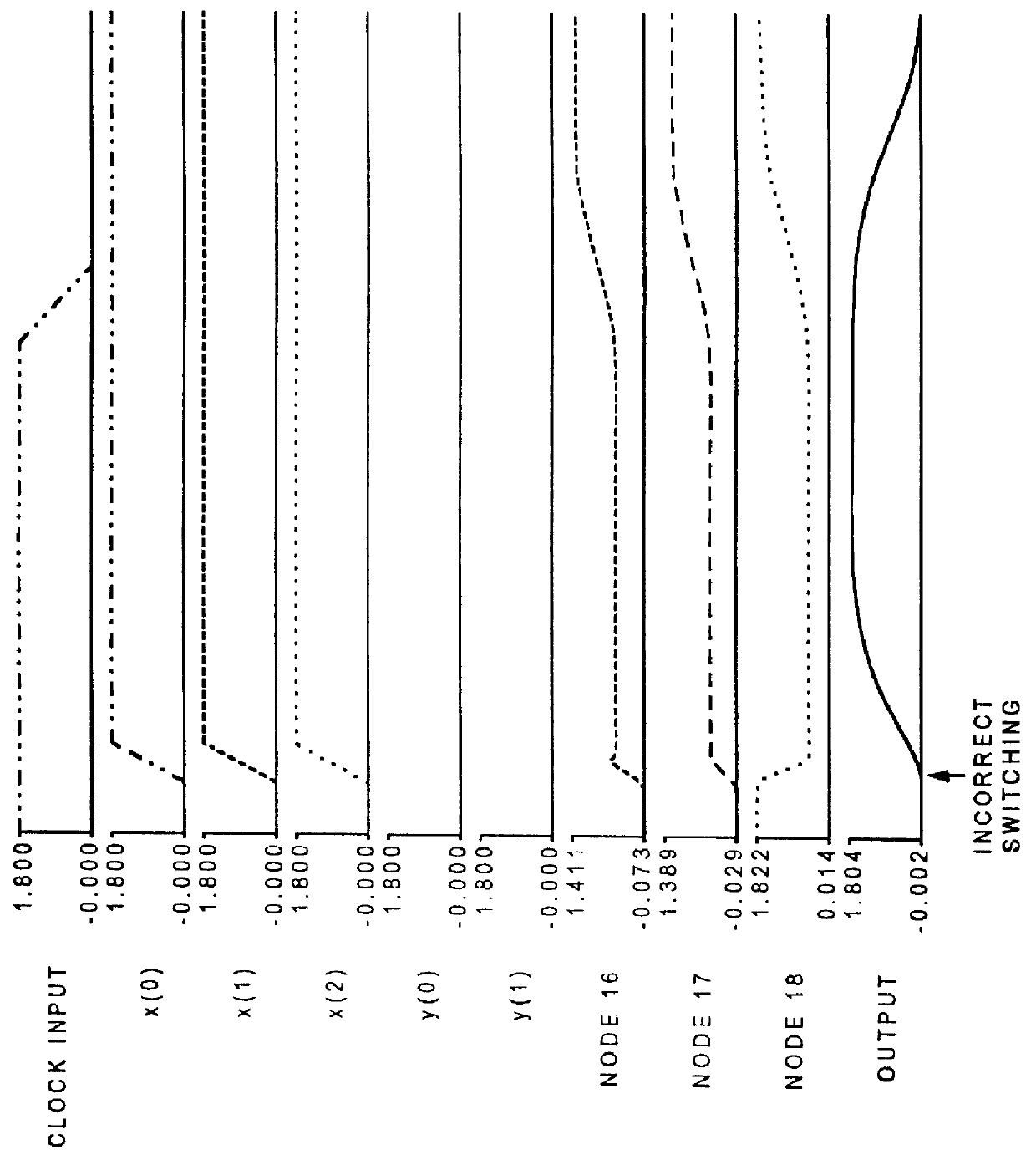
Referring now to the drawings and in particular to FIG. 1, there is depicted a circuit diagram of a conventional five-input complementary metal-oxide semiconductor (CMOS) domino logic circuit. As shown, domino logic circuit 10 includes input transistors 11-15. Input transistors 11-15 are generally n-channel enhancement mode devices (NMOS), each having a respective input x() or y(). When a logic high signal is applied to any one of inputs x() or y(), an associated one of input transistors 11-15 is turned on. In other words, a conduction channel is formed between the source and drain terminals of the respective input transistor.

An output indication of the conduction within some of input transistors 11-15 can be determined at node 18. Node 18 is also connected to a p-channel (PMOS) precharge transistor 21 having a drain connected to a supply voltage V.sub.dd. When precharge transistor 21 is driven into conduction by a logic low signal at its gate, the supply voltage V.sub.dd, coupled t...


PUM


Abstract

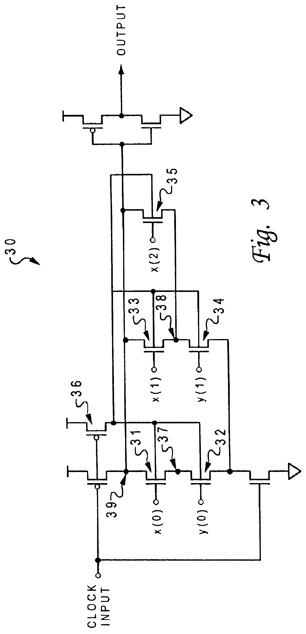
A domino logic circuit having a clocked precharge is disclosed. The domino logic circuit includes a precharge transistor, a discharge transistor, multiple input transistors, and a supplemental precharge transistor. Connected to a power supply, the precharge transistor receives a clock input. The discharge transistor is connected to ground and also receives the clock input. The input transistors, which are coupled between the precharge transistor and the discharge transistor, each receives a signal input. The supplemental precharge transistor is connected to the power supply and to a body of each of the input transistors. The supplemental precharge transistor also receives the same clock input as the precharge transistor.

Description

1. Technical FieldThe present invention relates to semiconductor circuits in general, and in particular to silicon on insulator semiconductor circuits. Still more particularly, the present invention relates to a silicon on insulator domino logic circuit.2. Description of the Prior ArtDomino logic circuits are commonly found in integrated circuits. A domino logic circuit simplifies digital logic by connecting a number of transistors together in series to implement digital combination logic. For example, a domino logic circuit implements a logic AND function by simply cascading a p-channel transistor with several n-channel input transistors in series. During operation, the p-channel transistor is clocked to precharge an output node of the circuit to a predetermined logic state. Depending on the logic state at the inputs of the n-channel input transistors, the output node either remains at its precharged state or is pulled low through the series of n-channel input transistors by a cloc...

Claims


Application Information

Patent Timeline
IPC IPC(8): H03K19/096
CPCH03K19/0963
Inventor DURHAM, CHRISTOPHER MCCALLKLIM, PETER GURSENPATEL, BINTA MINESH
Owner IBM CORP
Learn More