CMOS differential amplifier having offset voltage cancellation and common-mode voltage control

Inactive Publication Date: 2000-05-16
WSOU INVESTMENTS LLC +1
View PDF4 Cites 59 Cited by
  • Summary
  • Abstract
  • Description
  • Claims
  • Application Information

AI Technical Summary

Problems solved by technology

The problems associated with use of CMOS transistors as a differential pair lie in the offset voltage and in the common-mode voltage of each transistor.
However, due to various factors such as manufacturing variables, perfectly matched pairs of transistors are difficult to obtain, thus resulting in a non-zero value of V.sub.0 when the differential input signal is zero.
Such a condition detrimentally reduces the dynamic operat

Method used


Image

  • CMOS differential amplifier having offset voltage cancellation and common-mode voltage control
  • CMOS differential amplifier having offset voltage cancellation and common-mode voltage control
  • CMOS differential amplifier having offset voltage cancellation and common-mode voltage control

Examples


Embodiment Construction

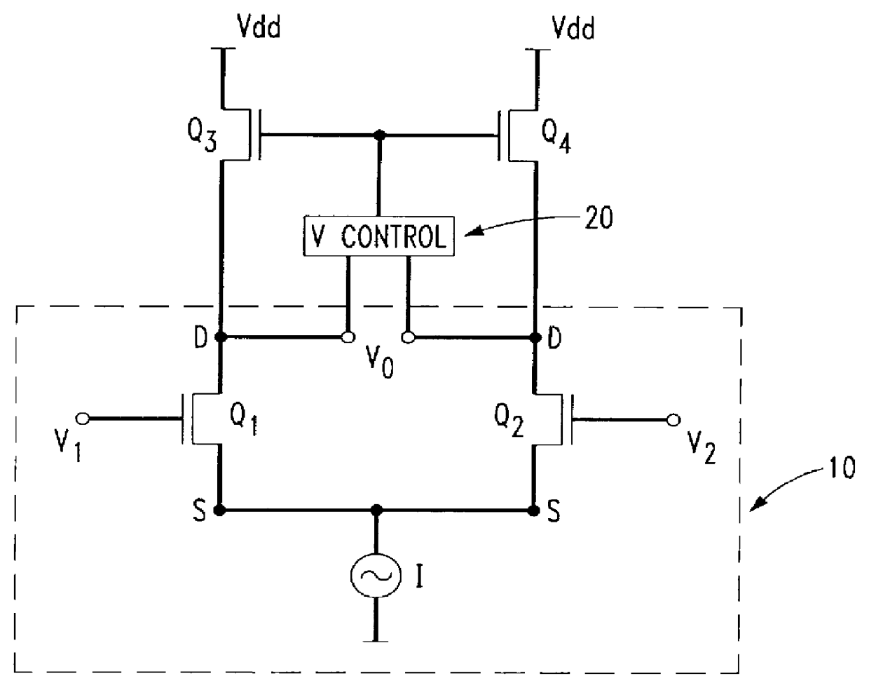
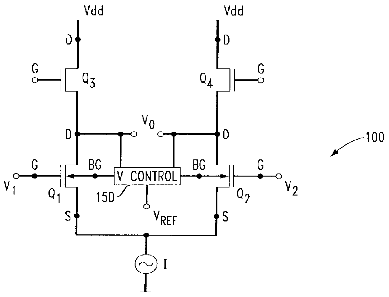
A differential amplifier circuit 100 constructed in accordance with the present invention is depicted in FIG. 2. Circuit 100 includes a pair of transistors Q.sub.1 and Q.sub.2, each having a base, a source, a drain and a backgate terminal and connected at the drain terminal to a DC current source (I) which provides a biasing quiescent current to the circuit. In the preferred embodiment, transistors Q.sub.1 and Q.sub.2 are CMOS transistors which, as is known in the art, are symmetrical devices. Thus, although current source I is shown connected to the source terminals, it could likewise be connected to the drain terminals. Biasing of the transistor pair Q.sub.1 and Q.sub.2 is completed through a pair of biasing transistors Q.sub.3, Q.sub.4, respectively, that are connected to a DC voltage source V.sub.dd. The transistors Q.sub.3, Q.sub.4 can be used as a load device or as an active transconductance device.

The transistors Q.sub.1 and Q.sub.2 of the amplifier circuit are operated as a ...


PUM


Abstract

A differential amplifier for amplifying the difference between first and second input signals and producing therefrom a differential output signal. The differential amplifier includes first and second transistors connected to a common DC current source and receiving, at the transistor gate terminals, the respective first and second input signals. Each transistor has a common mode voltage associated therewith. A voltage control circuit generates control signals that are applied to the backgate terminals of the transistors to calibrate the differential output voltage and to adjust the common mode voltages of the transistors.

Description

1. Field of the InventionThe present invention relates to operational amplifiers and, more particularly, to CMOS differential amplifiers having DC offset and common-mode voltage control.2. Background of Related ArtBalanced pairs of transistors, such as CMOS transistors, are often configured as differential pairs and used as common building blocks in amplifier design. In particular, such transistor pairs are typically employed in differential amplifiers to amplify the difference between two input signals. The problems associated with use of CMOS transistors as a differential pair lie in the offset voltage and in the common-mode voltage of each transistor.A known differential amplifier circuit 10 is schematically depicted in FIG. 1. The circuit 10 is constructed as a first a pair of transistors Q.sub.1 and Q.sub.2 connected to a DC current source I and connected to a second pair of transistors Q.sub.3, Q.sub.4 that may function as a load and / or as a transconductance element, as is kno...

Claims


Application Information

Patent Timeline
IPC IPC(8): H03F3/45
CPCH03F3/45654H03F2203/45342
Inventor WANG, HONGMO
Owner WSOU INVESTMENTS LLC
Why Eureka
Try Eureka