Variable impedance output driver circuit using analog biases to match driver output impedance to load input impedance

a driver circuit and variable impedance technology, applied in logic circuits, pulse techniques, reliability increasing modifications, etc., can solve the problems of limited turn-on/turn-off staggering, inability to adjust the impedance of the driver, and the driver provides minimal control of the switching current characteristics

Inactive Publication Date: 2000-10-17
IBM CORP
View PDF15 Cites 71 Cited by
  • Summary
  • Abstract
  • Description
  • Claims
  • Application Information

AI Technical Summary

Problems solved by technology

The driver impedance requirements result in "programmable impedance" drivers whose output resistance is varied using complicated digital controls.
First, to achieve fine impedance resolution, many FET controls must be applied to every driver, representing a significant amount of wiring.
Because any bina

Method used


Image

  • Variable impedance output driver circuit using analog biases to match driver output impedance to load input impedance
  • Variable impedance output driver circuit using analog biases to match driver output impedance to load input impedance
  • Variable impedance output driver circuit using analog biases to match driver output impedance to load input impedance

Examples


Embodiment Construction

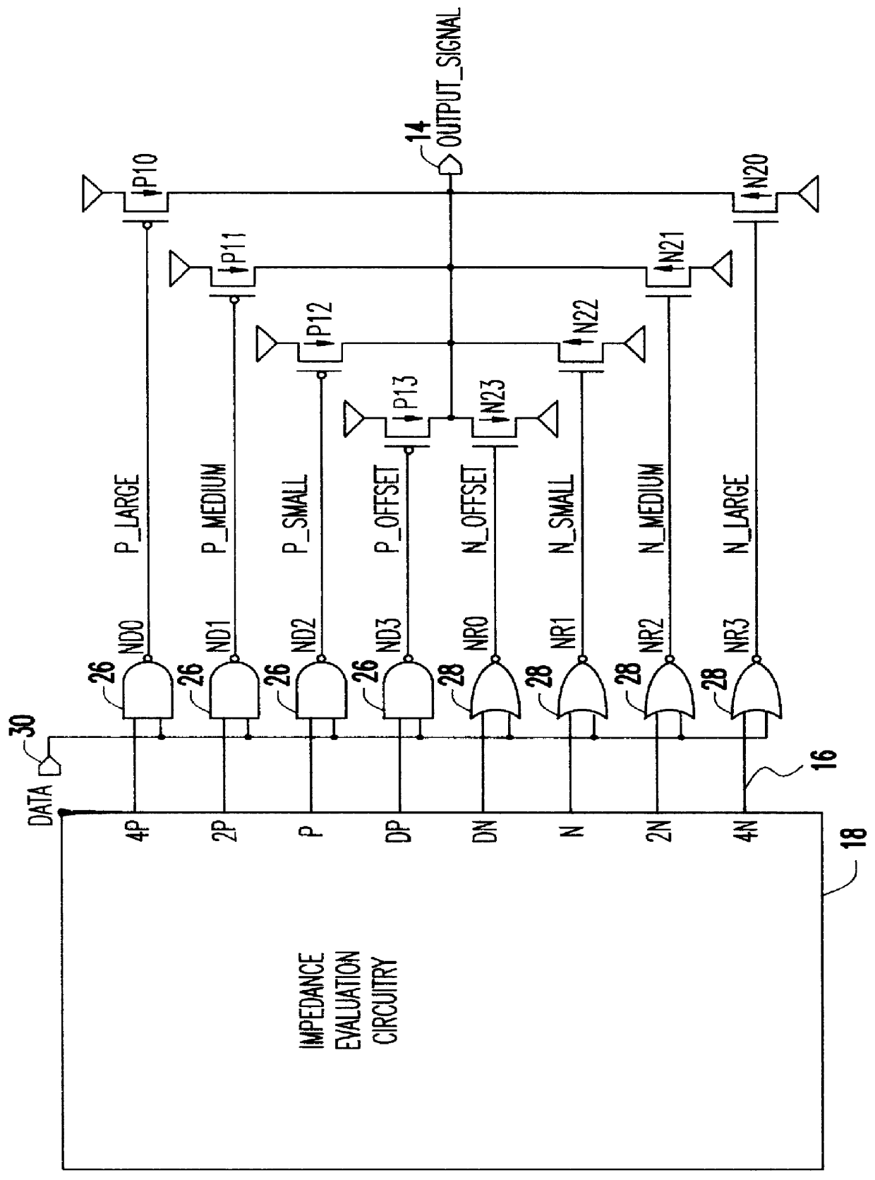
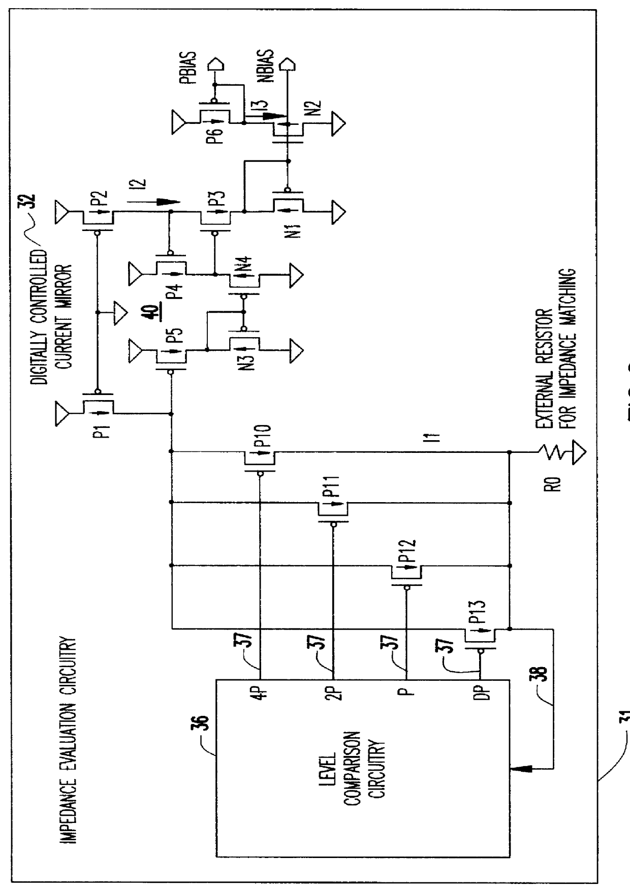
Referring now to the drawings, and more particularly to FIG. 2, there is shown an impedance evaluation circuit 31 according to the present invention wherein a digitally controlled current mirror 32 is used to obtain a measurement of an external resistance value R.sub.Q 34 for matching the impedance of a driven load. The current mirror 32 comprises two back-to-back PFET transistors, P1 and P2, connected at their gates to ground and their drains connected to a supply voltage. With this arrangement, the current I1 flowing through P1 in a first leg of the current mirror matches the current I2 flowing in P2, a second leg of the current mirror, provided P1-and P2 have identical characteristics. The level comparison circuitry 36 selects several of "n" PFET fingers P10-P13 using a binary combination of the available control signals. The selected PFET fingers P10-P13 combine with P1 of the current mirror 32 to determine the amount of current I1 through the external resistor R.sub.Q 34. The l...


PUM


Abstract

A programmable variable impedance output driver circuit uses analog biases to match driver output impedance to load input impedance. A current mirror is used to obtain a measurement of an external resistance value for matching the impedance of a driven load. The mirrored current generates the voltage "NBIAS" when passed through the resistively connected NFET. Similarly, the current is again mirrored and passed through a resistively connected PFET resulting in the voltage "PBIAS". The analog bias voltages, NBIAS and PBIAS are used to vary the impedance of complementary FETs in an impedance matched driver for a high degree of dI/dt control. The driver provides a high degree of flexibility because its turn-on and turn-off characteristics do not depend on a combination of digital control signals connected directly to the driving FETs as in the prior art. Instead, the PBIAS and NBIAS signals provide analog controls which may be applied to single transistors whose impedance changes as PBIAS and NBIAS increase or decrease.

Description

1. Field of the InventionThe present invention generally relates to output driver circuits and, more particularly, to a programmable variable impedance output driver circuit which uses analog biases to match driver output impedance to load input impedance.2. Description of the Related ArtIn electronic systems, output drivers are required to drive I / O (input / output) devices and similar loads. In order to have efficient power transfer it is important that the impedance of the driver closely match the impedance of the load; the load comprising the impedance of the driven device as well as the impedance of the transmission line. Ideally, the driver impedance and the load impedance are equal. High performance output driver circuits require careful control of both current switching and output impedance characteristics. The former requirement, commonly referred to as dI / dt control, requires switching the driver on over a specified period of time, or switching multiple stages of the driver ...

Claims


Application Information

Patent Timeline
IPC IPC(8): H03K19/00
CPCH03K19/0005
Inventor HANSEN, PATRICK R.PILO, HAROLD
Owner IBM CORP
Why Eureka
Try Eureka