Polishing apparatus and polishing method

a technology of polishing apparatus and polishing method, which is applied in the direction of lapping machines, manufacturing tools, instruments, etc., can solve the problems of low alignment accuracy of cmp apparatus, inability to accurately measure a location, and inability to accurately measure the thickness of the material to be polished

Inactive Publication Date: 2000-11-07
CANON KK
View PDF14 Cites 64 Cited by
  • Summary
  • Abstract
  • Description
  • Claims
  • Application Information

AI Technical Summary

Problems solved by technology

However, the CMP apparatus described above is incapable of measuring a thickness of a material to be polished, modifying polishing conditions on the basis of a measured results and polishing the material with high precision in a short time since the conventional thickness measuring means requires a long time to align the location at which a thickness is to be measured of the surface of the material to be polished.
Further, the CMP apparatus has a low alignment accuracy, thereby being hardly capable of accurately measuring a location at which a thickness is to be measured.
Accordingly, obtained thickness values have low reliabilities and are hardly usable as data for modifying polishing conditions.

Method used


Image

  • Polishing apparatus and polishing method
  • Polishing apparatus and polishing method
  • Polishing apparatus and polishing method

Examples


Embodiment Construction

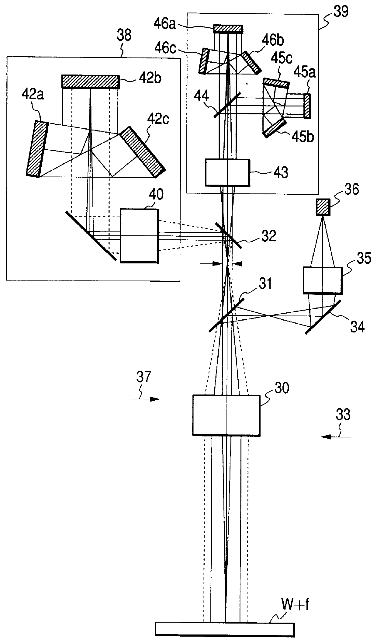
In the example of the present invention, a material to be polished is polished by a polishing process which is divided sequentially into a coarse polishing step (S1), thickness measuring steps (S2 to S8) and finish polishing steps (S9 to S11) by using the polishing apparatus of the fifth embodiment, as shown in a flowchart of FIG. 22.

The material to be polished 1 which has been coarsely polished in the coarse polishing unit 21 in the coarse polishing step (S1) is conveyed by a conveying means (not shown in the drawings) to the thickness measuring unit and held therein (S2) by a holding means 2 for the material to be polished. Then, the thickness measuring means 7 shifts right over the location W1 of a wafer shown in FIG. 21C (S3). When the film measuring means 7 locates itself right over the location W1, the momentary white light source glows (S4), whereby image information is obtained from reflected rays with the location W1 as a center of a light bundle (S5). On the basis of the o...


PUM

PropertyMeasurementUnit
angleaaaaaaaaaa
daaaaaaaaaaa
diameteraaaaaaaaaa

Abstract

In order to measure a thickness of a surface to be polished of a material to be polished for a short time, two-dimensional images are obtained from a light reflected from the surface to be polished of the material to be polished, a location at which a thickness is to be observed is specified by the obtained two-dimensional images, and thickness measurement is carried out.

Description

1. Field of the InventionThe present invention relates to a polishing apparatus which has observing means for observing a surface of a material to be polished and a polishing method of polishing a material to be polished using the polishing apparatus.2. Related Background ArtIn the recent years where progresses have been made in configuration of ultra fine semiconductor devices and sophisticatedly stepped semiconductor devices, chemical-mechanical polishing (CMP) apparatuses are known as a working means for polishing with high precision, SOI substrates, semiconductor wafers made of Si, GeAs, InP and the like, wafers having insulating films or metal films formed on surfaces thereof in processes of manufacturing integrated semiconductor circuits, and substrates for displays.A CMP apparatus which was used by the inventors before achieving the present invention will be described with reference to FIG. 23. FIG. 23 schematically shows the polishing apparatus which was used by the inventor...

Claims


Application Information

Patent Timeline
Patent Type & Authority Patents(United States)
IPC IPC(8): B24B37/04B24B49/12B24B37/013
CPCB24B49/12B24B37/013
Inventor NYUI, MASARUBAN, MIKICHISUZUKI, TAKEHIKOSUGIYAMA, YASUSHI
Owner CANON KK
Why Eureka
Try Eureka