

Copper contamination control of in-line probe instruments
a probe instrument and probe technology, applied in the direction of instruments, chemistry apparatus and processes, cleaning using tools, etc., can solve the problems of copper contamination during various phases of chip fabrication, silicon can easily lose its critical effective properties, and the potential for copper contamination raises a host of technical and logistical problems
- Summary
- Abstract
- Description
- Claims
- Application Information
AI Technical Summary
Benefits of technology
Problems solved by technology
Method used
Image

Examples
Embodiment Construction
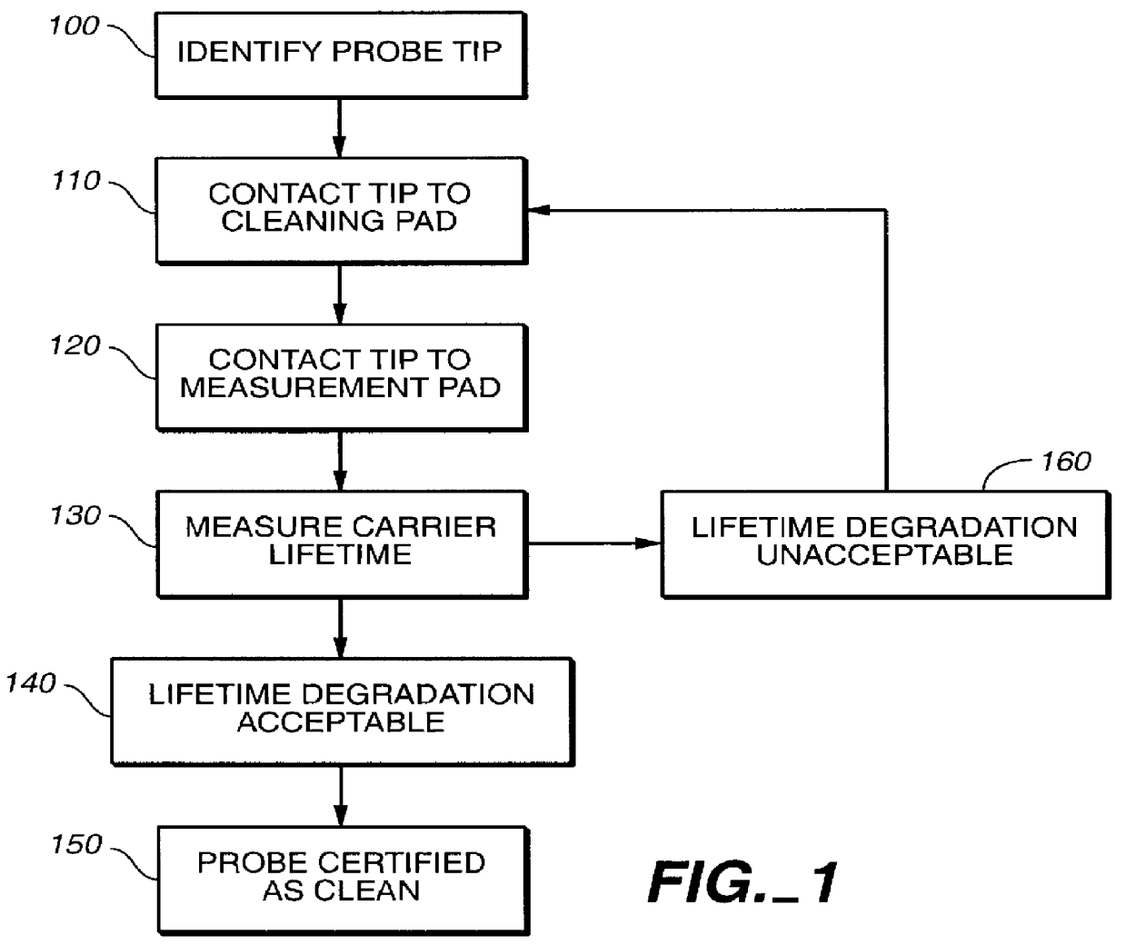
FIG. 1 is a flow chart illustrating the overall method of the invention. The first step involves identifying the probe tip to be cleaned and tested (Step 100). This might involve identifying a tool probe tip that has been used in physical contact with metal layers during chip testing or which has not been confirmed to be free of copper contamination prior to use in a testing application. The probe tip identified could be a component of any number of metrology tools used in the integrated circuit fabrication process, such as test probes manufactured by Keithley or test probes manufactured by Electroglass.
The next step in the method involves placing the probe tip in physical contact with a cleaning pad (step 110). This cleaning pad is comprised of any material that demonstrates the ability to remove copper contamination from the tip of the probe tool. For example, it has been demonstrated that a wafer of silicon will remove copper contamination from the tip of metrology probe tool if ...
PUM
 Abstract
Description
Claims
Application Information