Field emission display

a field emission display and display technology, applied in the direction of discharge tube main electrodes, discharge tube luminescnet screens, discharge tube with screens, etc., can solve the problems of high vacuum inside the structure, interference with cathode formation and placement, and difficulty in fabricating spacers

Inactive Publication Date: 2001-01-09
MICRON TECH INC
View PDF32 Cites 77 Cited by
  • Summary
  • Abstract
  • Description
  • Claims
  • Application Information

AI Technical Summary

Problems solved by technology

One problem with a device such as this is the maintenance of the required parallel spacing between the cathode plate and the faceplate.
This problem is the result of the high vacuum inside the structure.
While effective, such spacers are difficult to fabricate and interfere with cathode formation and placement.
Another problem with using a silicon backplate or cathode plate in conjunction with a glass faceplate is the difficulty of forming an adequate seal between the silicon and the glass for purposes of maintaining a vacuum within the displa...

Method used


Image

  • Field emission display
  • Field emission display
  • Field emission display

Examples


Embodiment Construction

This disclosure of the invention is submitted in furtherance of the constitutional purposes of the U.S. Patent Laws "to promote the progress of science and useful arts." U.S. Constitution, Article 1, Section 8.

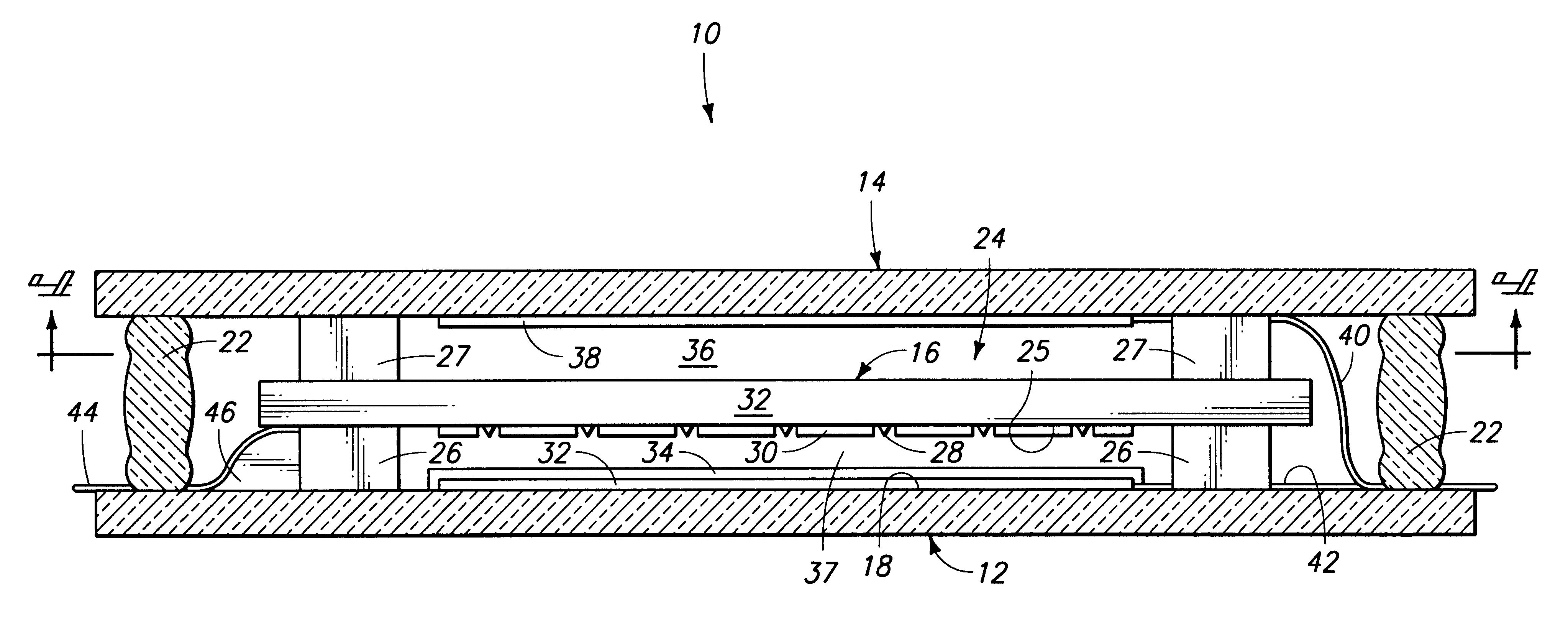
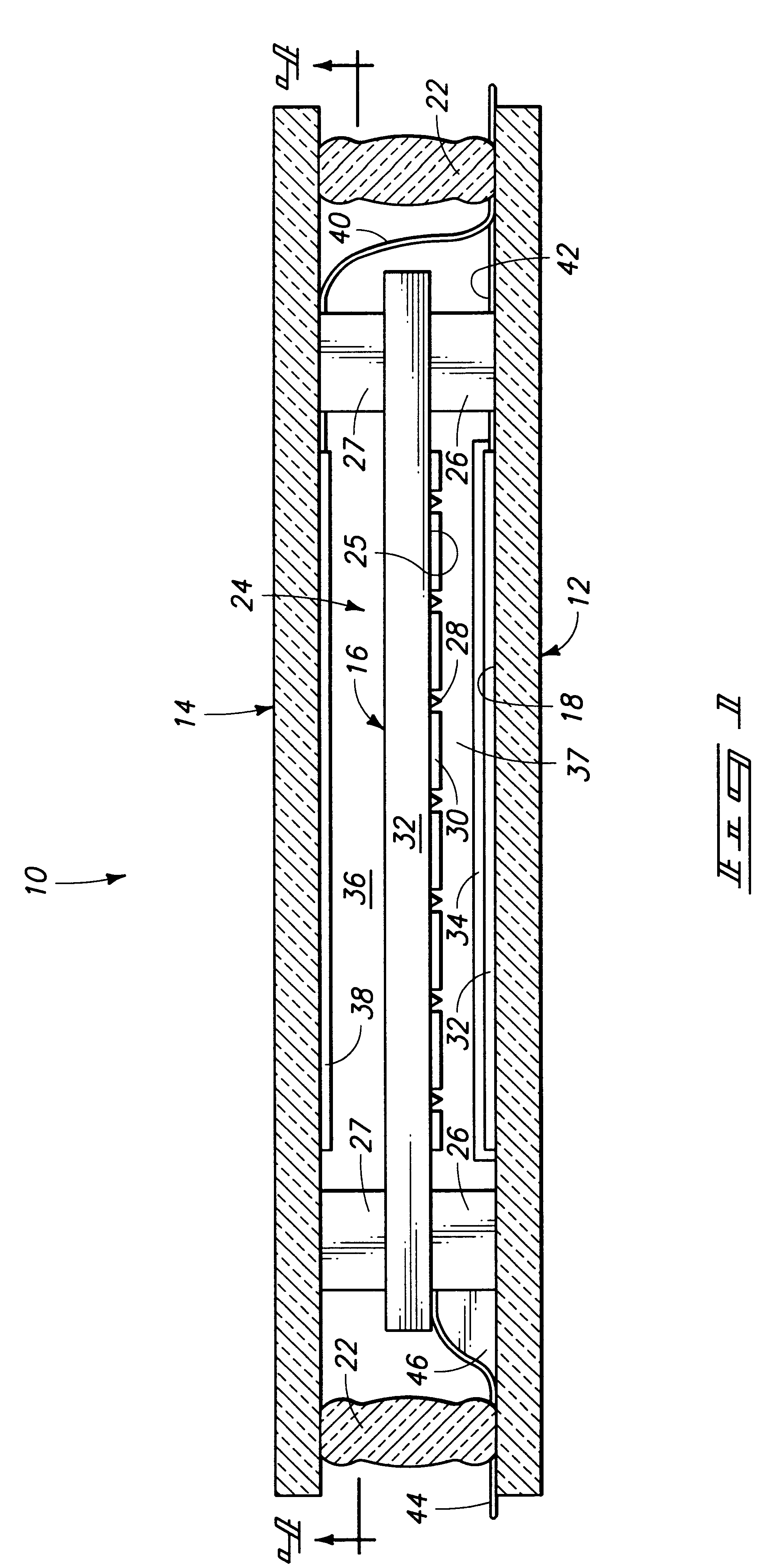
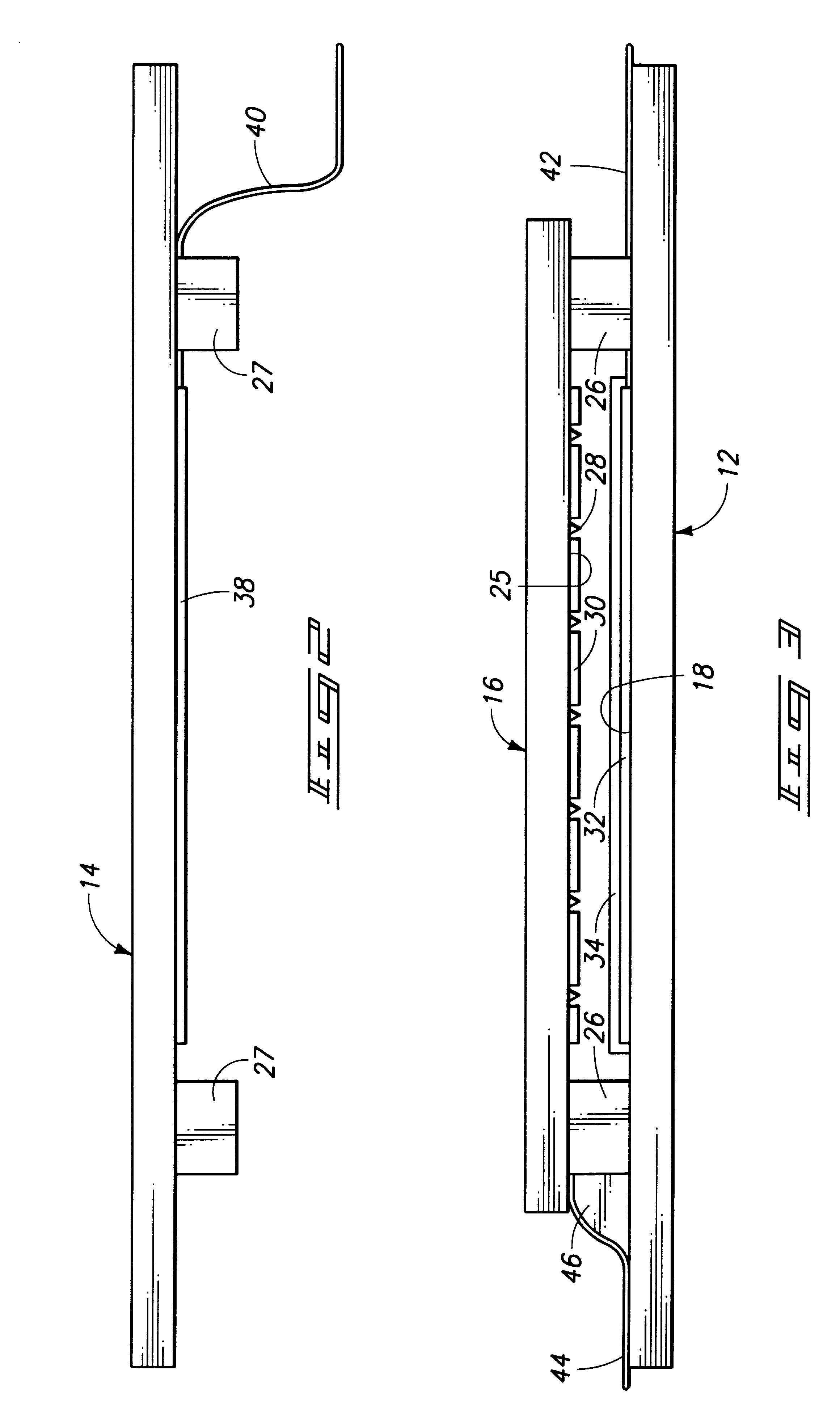
FIGS. 1-4 show components of a flat-panel field emission display 10 in accordance with a preferred embodiment of the invention. It is to be understood that the drawings are not to scale. They have been simplified to illustrate the novel features of the invention and its constituent parts. Some features of the preferred embodiment are also described in two concurrently-filed applications, both assigned to Micron Display Technology, Inc., entitled "Multilayer Electrical Interconnection Structures and Fabrication Methods" and "Methods of Mechanical and Electrical Substrate Connection," the disclosures of which are hereby incorporated by reference.

Flat-panel display 10 generally includes a transparent faceplate 12, a backplate 14, and a cathode plate 16 positioned between faceplat...


PUM


Abstract

A flat-panel field emission display comprises a luminescent faceplate, a rigid backplate, and an interposed or sandwiched emitter or cathode plate. A positioning spacer or connector ridge is formed on the rear surface of the faceplate to space the cathode plate a fixed distance behind the faceplate. A peripheral seal is formed between the faceplate and the backplate. The faceplate, backplate, and peripheral seal define an evacuated internal space which contains the cathode plate. The backplate is spaced behind the cathode plate to create a rearward vacuum space in which a getter is located.

Description

TECHNICAL FIELDThis invention relates flat-panel field emissions displays.BACKGROUND OF THE INVENTIONFlat-panel displays are widely used to visually display information where the physical thickness and bulk of a conventional cathode ray tube is unacceptable or impractical. Portable electronic devices and systems have benefitted from the use of flat-panel displays, which require less space and result in a lighter, more compact display system than provided by conventional cathode ray tube technology.The invention described below is concerned primarily with field emission flat-panel displays. In a field emission flat-panel display, an electron emitting cathode plate is separated from a display face or faceplate at a relatively small, uniform distance. The intervening space between these elements is evacuated. Field emission displays have the outward appearance of a CRT except that they are very thin. While being simple, they are also capable of very high resolutions. In some cases they...

Claims


Application Information

Patent Timeline
IPC IPC(8): H01J29/94H01J29/00H01J31/12H01J29/90
CPCH01J29/90H01J29/94H01J31/127H01J2329/8625H01J2329/92
Inventor CATHEY, DAVID A.WATKINS, CHARLES
Owner MICRON TECH INC
Why Eureka
Try Eureka