

Method of producing semiconductor device comprising insulation layer having improved resistance and semiconductor device produced thereby
a technology of insulation layer and semiconductor, which is applied in the direction of semiconductor device, semiconductor/solid-state device details, electrical apparatus, etc., can solve the problems of loss of electrical continuity, defective electrical continuity between them, and breakage of some of the bonds between atoms in the polyimide layer, and loss of insulation properties
Inactive Publication Date: 2001-03-13
SHINKO ELECTRIC IND CO LTD
View PDF4 Cites 126 Cited by
- Summary
- Abstract
- Description
- Claims
- Application Information
AI Technical Summary
Problems solved by technology
The presence of such an oxidized film is not preferable in that it increases a contact resistance between the electrode or pad and wiring line to be connected with it, and eventually makes electrical continuity between them defective.
However, such an ion bombardment simultaneously has also effect on the surface of the polyimide layer as an insulation film exposed at the top of the wafer, resulting in breakage of some of bonds between atoms in the polyimide layer and loss of its insulation properties.
Such a problem is not desired in a semiconduct
Method used
View moreImage
Smart ImageViewing Examples

Examples
 PUM
 Abstract
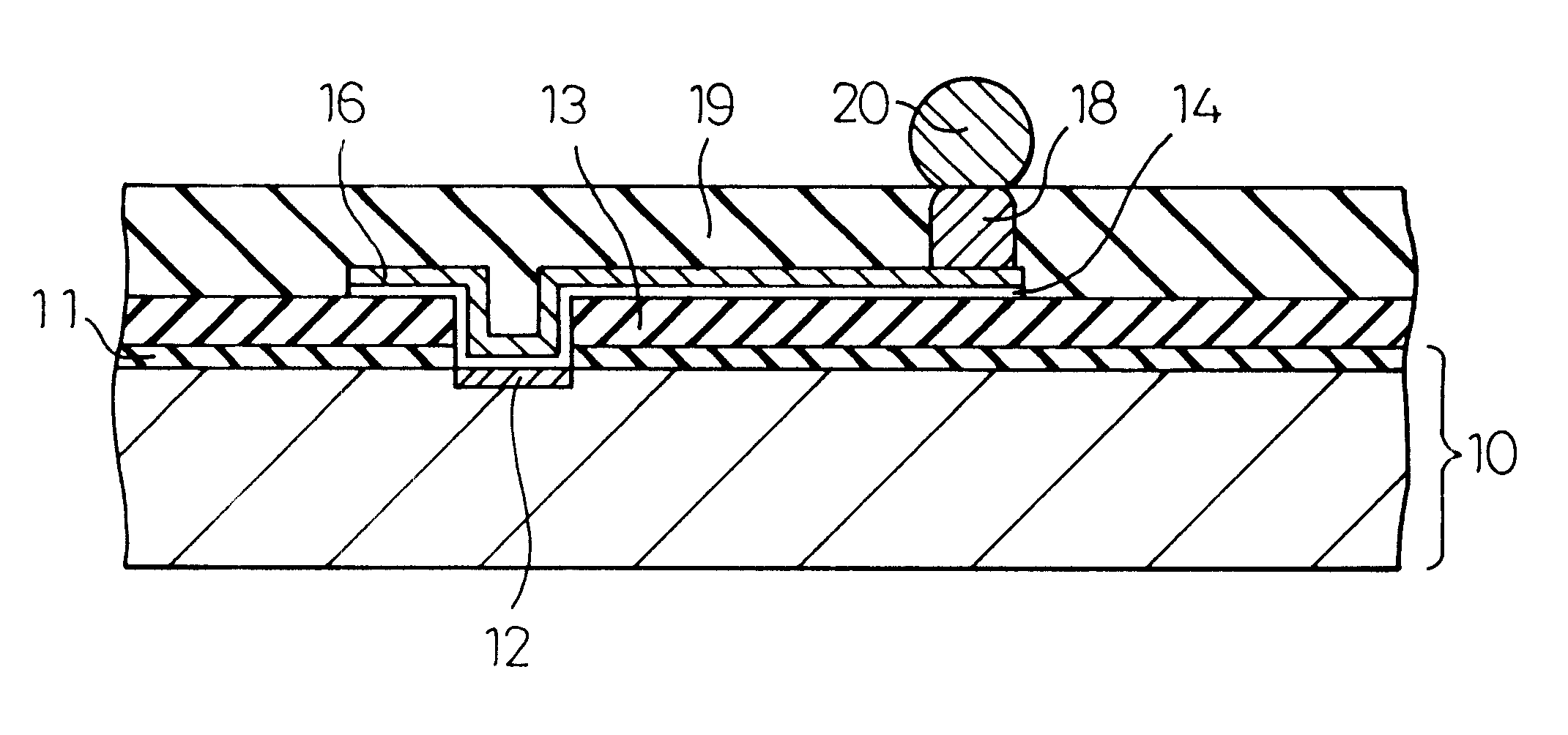
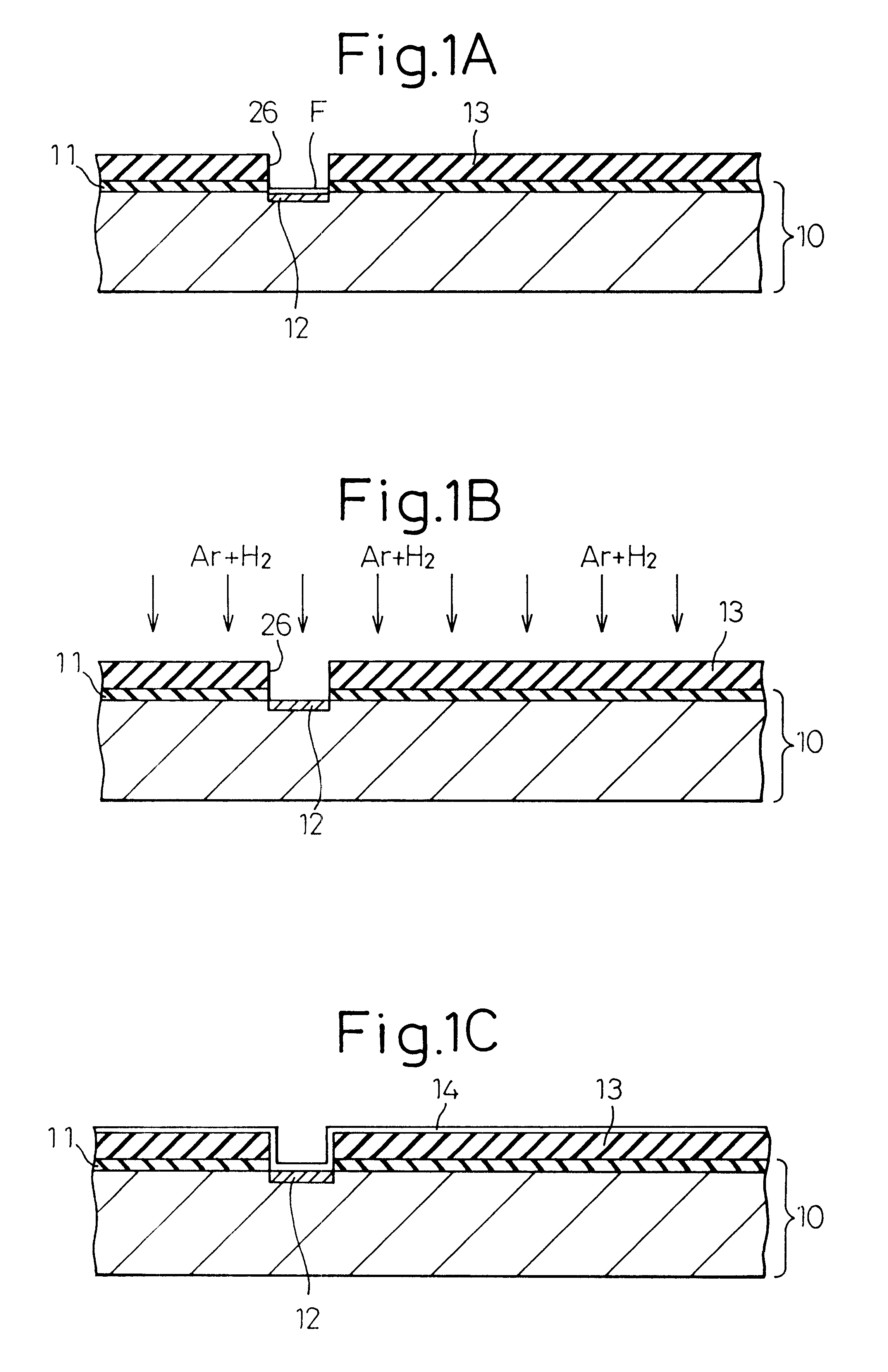
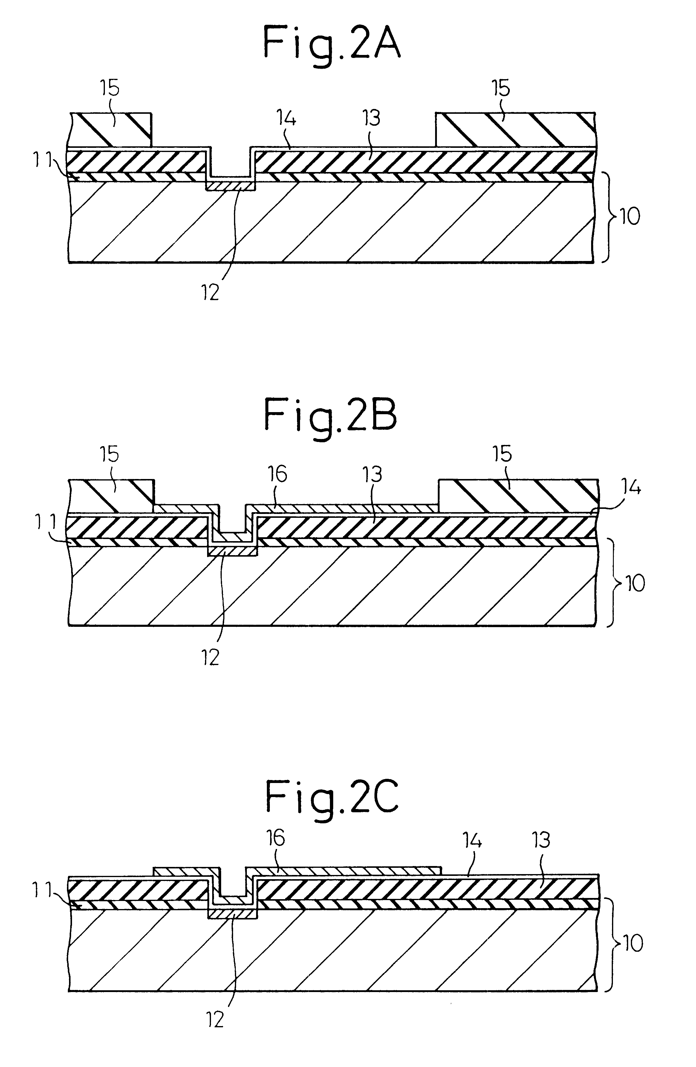
A semiconductor device comprising an insulation film covering a semiconductor chip so as to expose electrodes or pads fabricated in the chip and wiring lines located on the insulation film and connected to the respective electrodes or pads is produced by a method which comprises: providing a semiconductor chip provided with an insulation film covering the chip so as to expose a conductor layer for electrodes or pads fabricated in the chip, ion milling the surface of the chip provided with the insulation film by a mixed gas of argon and hydrogen, forming a patterned conductor layer for wiring lines on the ion-milled surface of the chip, and dry etching the surface of the chip provided with the insulation film and the patterned conductor layer by nitrogen gas.
Description
1. Field of the InventionThe invention relates to a semiconductor device and a method of producing the same. Particularly, the invention relates to a semiconductor device, such as one having a chip size package (CSP) structure, in which a surface of the semiconductor chip is covered by a layer of insulation material, such as a layer of polyimide, and a layer of aluminum (Al) forming electrodes or pads at the surface of the chip is not covered by the insulation material layer and is exposed.As used herein, the term "semiconductor chip" means each of the individual semiconductor elements which are fabricated in a wafer and are not yet cut from the wafer as well as each of individual semiconductor elements which are cut from the wafer and separated from each other, unless specifically indicated.2. Description of the Related ArtIn a typical and conventional semiconductor device, an Al layer, which provides electrodes, is formed on a chip of silicon (Si), and it is common that wiring lin...
Claims
Login to View More Application Information
Patent Timeline
 IPC IPC(8): H01L21/02H01L21/70H01L21/768H01L21/60
CPCH01L21/76814H01L23/3107H01L24/03H01L24/05H01L24/11H01L24/12H01L2224/04042H01L2224/48647H01L2224/48624H01L2924/01024H01L24/45H01L2924/05042H01L2924/014H01L2924/01079H01L2924/01078H01L2224/0231H01L2224/0401H01L2224/05624H01L2224/05647H01L2224/1147H01L2224/13099H01L2224/45144H01L2924/01006H01L2924/01007H01L2924/01011H01L2924/01013H01L2924/01014H01L2924/01018H01L2924/01027H01L2924/01028H01L2924/01029H01L2924/01033H01L2924/01075H01L2924/00014H01L2924/00H01L2224/11334H01L2924/12042H01L23/3114H01L21/32135H01L21/32139H01L21/76883
InventorITO, DAISUKEKITAHARA, YUICHI
OwnerSHINKO ELECTRIC IND CO LTD