Bootstrapped low-voltage switch

a low-voltage switch and bootstrap technology, applied in the direction of pulse technique, process and machine control, instruments, etc., can solve the problems of gate oxide becoming increasingly sensitive, significant signal distortion, and ratios supposedly continuing to decreas

Inactive Publication Date: 2001-04-10
ANALOG DEVICES BV
View PDF8 Cites 32 Cited by
  • Summary
  • Abstract
  • Description
  • Claims
  • Application Information

AI Technical Summary

Problems solved by technology

This effect can cause significant signal distortion.
As the technologies are scaled down, the gate oxide becomes increasingly sensitive.
This ratio w

Method used


Image

  • Bootstrapped low-voltage switch
  • Bootstrapped low-voltage switch
  • Bootstrapped low-voltage switch

Examples


Embodiment Construction

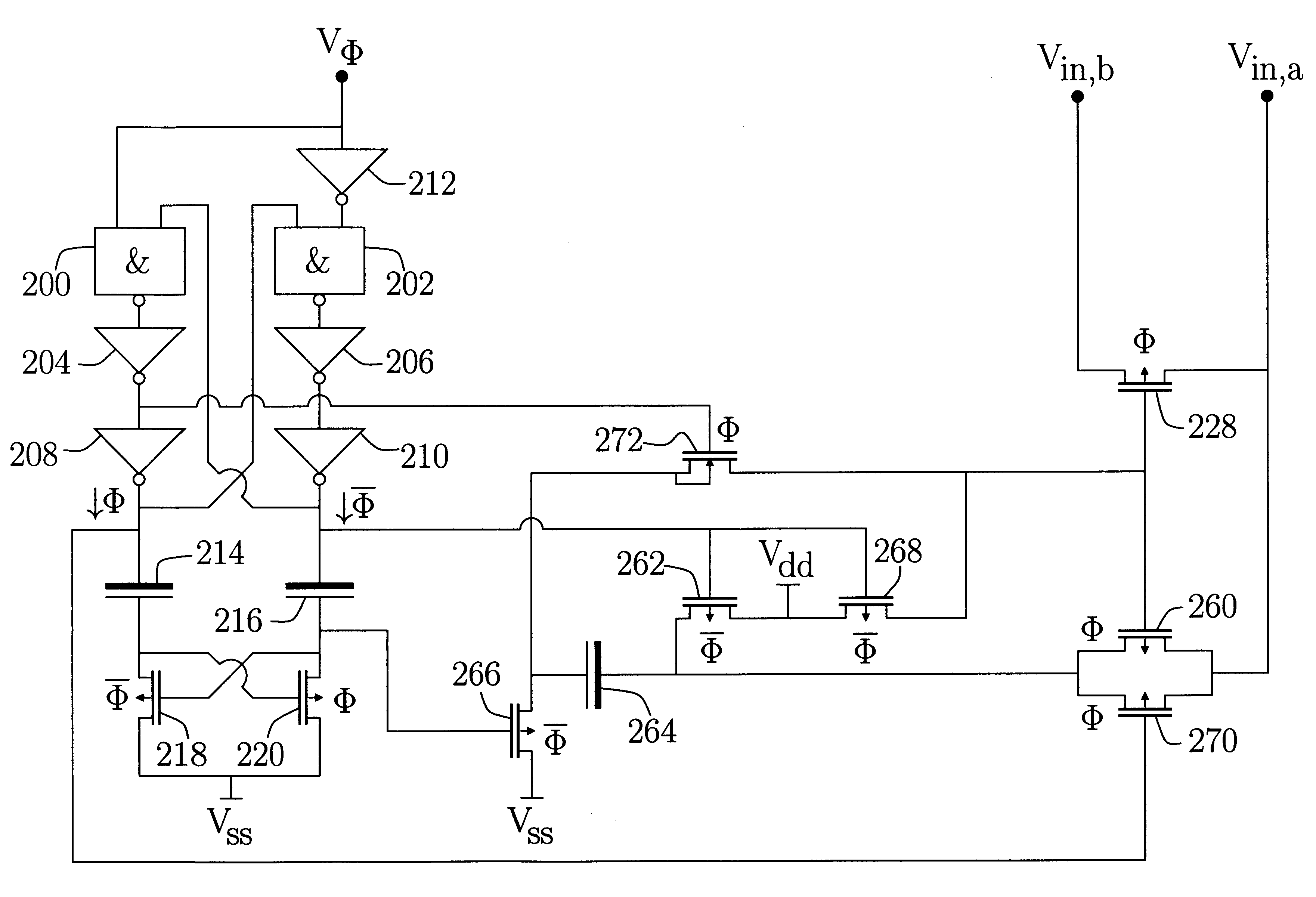
FIGS. 5A, 5B, 5C, 6A, 6B, 6C, and 6D shows some preferred embodiments. They are all designed for implementation in CMOS P-well technologies providing enhancement-mode MOSFETs. Thus, all P-channel MOSFETs (PMOS) have their "bulk terminal" connected to a common substrate. It is assumed that the common substrate is connected to the high supply potential V.sub.dd.

MOSFETs are usually symmetrical with respect to their drain and source terminals. In the following description, the term "drain terminal" has randomly been assigned to one of the two terminals (the other being the "source terminal"). The distinction is made merely to provide clarity. Minor improvements may possibly be obtained by using asymmetrical MOSFETs.

For simplicity, it is assumed that the absolute value of the threshold voltage of a PMOS is approximately the same as the threshold voltage of a NMOS. In this patent application, the term "threshold voltage" refers to the absolute value, regardless of the polarity of the tran...


PUM


Abstract

A low-voltage constant-impedance analog switch based on a single MOSFET [328] as the main switching element. The constant-impedance on-state operation is obtained by connecting a charged capacitor [326] between the gate and source terminals of the MOSFET [328]. The switch can be compensated for the body effect, which may be necessary to obtain the required level of linearity. Low-voltage operation is made feasible by employing an internal feedback loop that locks in the switch's on-state. The switch can be implemented in a single-well CMOS bulk technology, and it can operate at supply-voltage differences that are only slightly higher than the technology's threshold voltage.

Description

This invention relates to switches for use in partly-analog integrated circuits. More particularly, this invention relates to low-voltage analog switches operating with constant overdrive.2 BACKGROUND: DESCRIPTION OF PRIOR ARTAnalog switches are used in various electrical circuits such as: multiplexers, sample-and-hold (S / H) circuits, analog-to-digital converters (ADCs), digital-to-analog converters (DACs), and in particular in discrete-time analog systems such as switched-capacitor (SC) and switched-current (SI) circuits.2.1 An Analog SwitchAn analog switch is a controllable two-terminal device as illustrated in FIG. 1. It will typically have two states: an "on-state" and an "off-state." In the on-state, the analog switch should short circuit the two switch terminals, labeled V.sub.in,a and V.sub.in,b in the Figures. In the off-state, the analog switch should disconnect the two switch terminals. In neither state should the analog-switch circuit load the switch terminals. The state ...

Claims


Application Information

Patent Timeline
IPC IPC(8): H03K17/06
CPCH03K17/063H03K2217/0018
Inventor STEENSGAARD-MADSEN, JESPER
Owner ANALOG DEVICES BV
Why Eureka
Try Eureka