

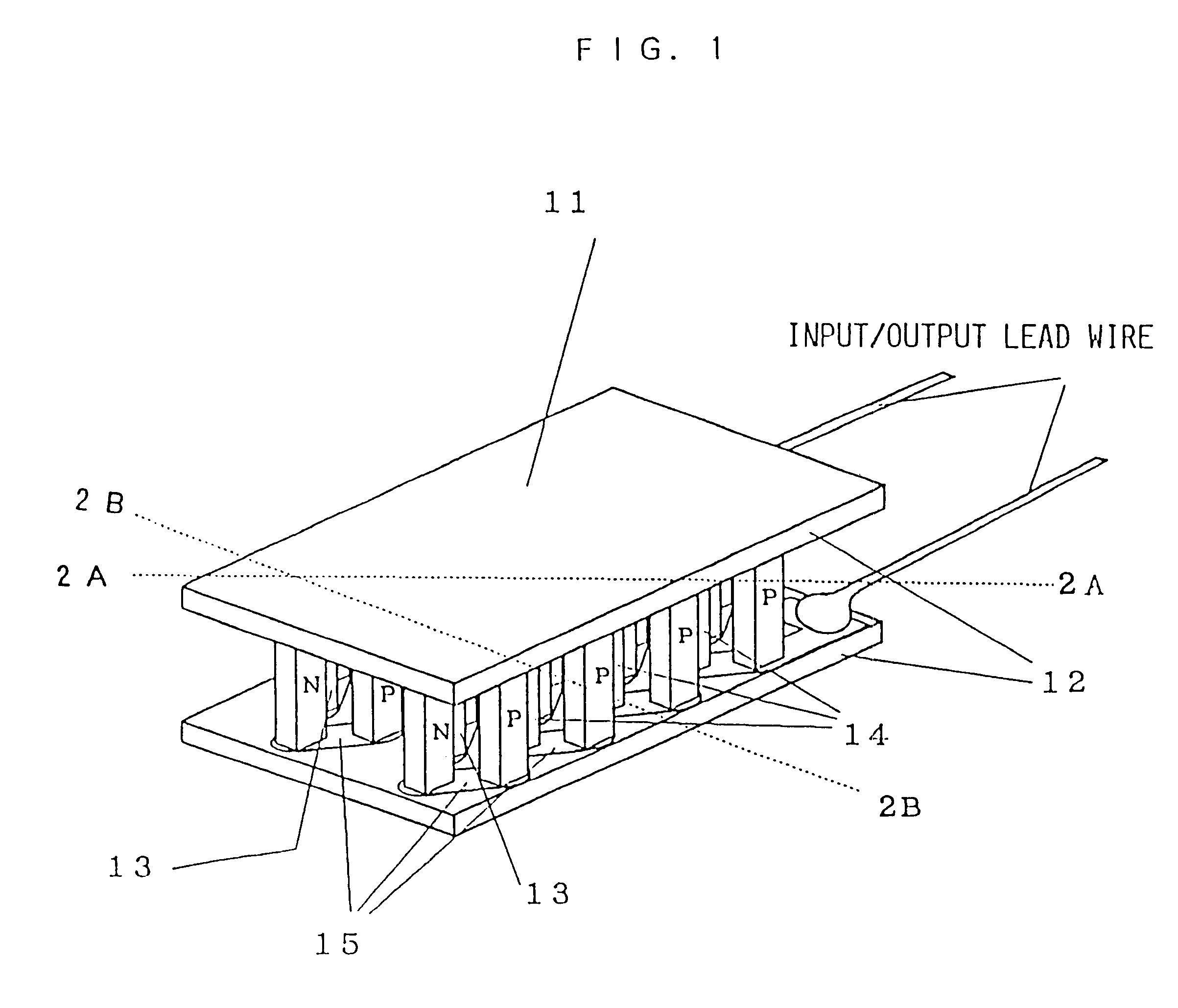
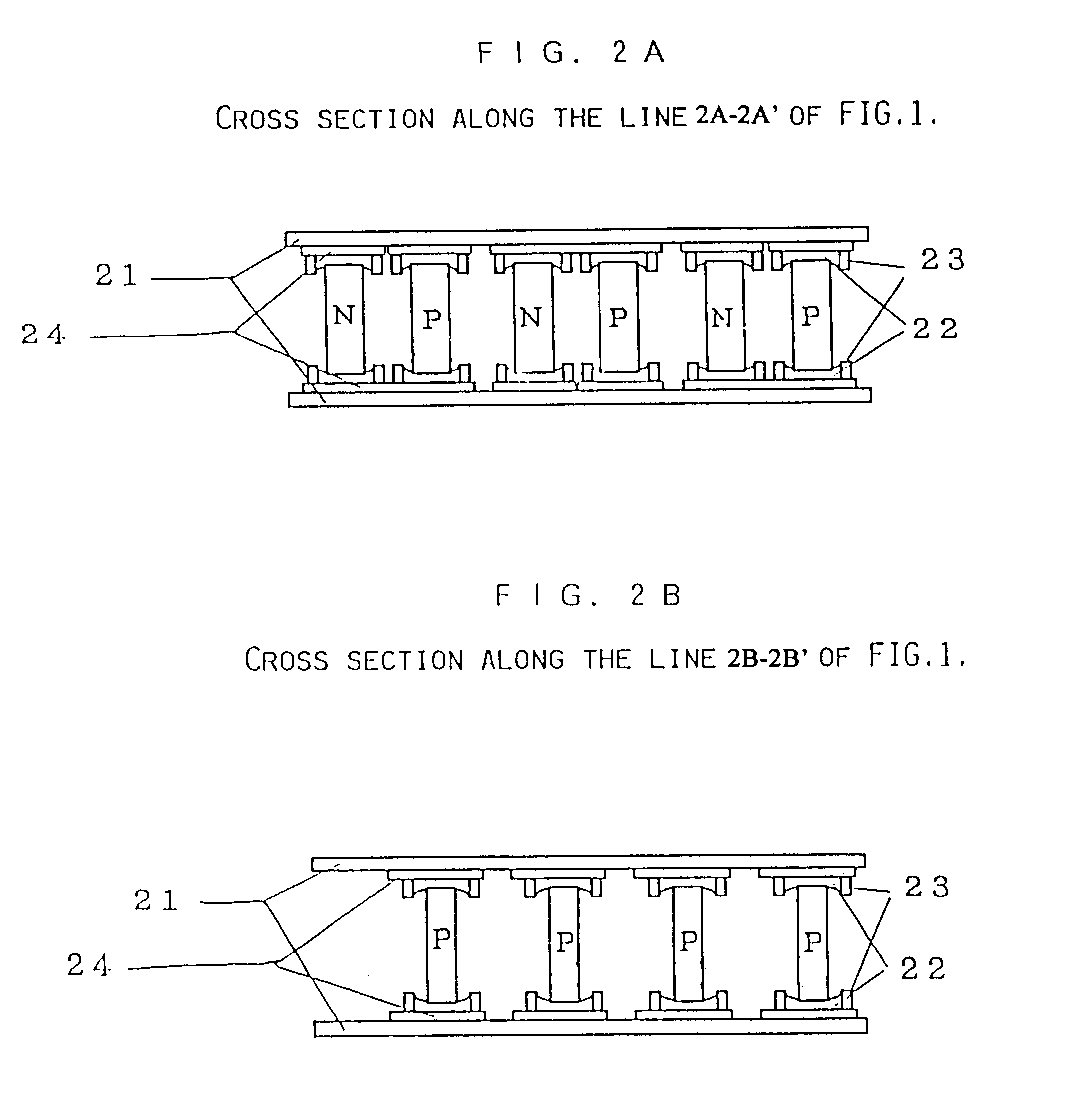
Thermoelectric device
a technology of thermoelectric devices and thermoelectric materials, which is applied in the manufacture/treatment of thermoelectric devices, semiconductor devices, electrical apparatus, etc., can solve the problems of difficult handling of thermoelectric materials, limited reduction of chip size and device size considering operation performance and working accuracy, and difficulty in making thermoelectric devices having the conventional structur
- Summary
- Abstract
- Description
- Claims
- Application Information
AI Technical Summary
Problems solved by technology
Method used
Image

Examples
embodiment-4
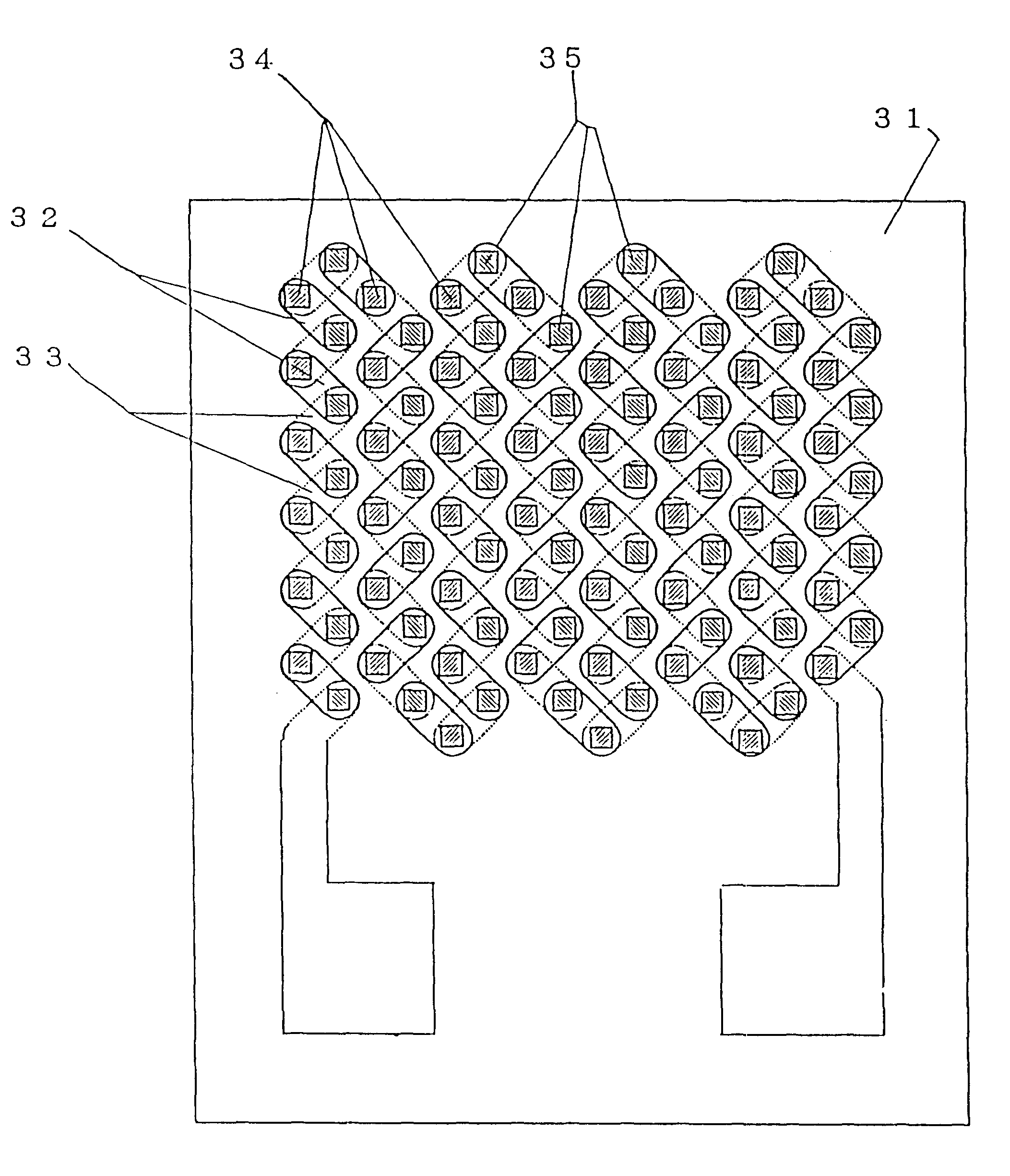
As explanation will be given of making a small-scaled thermoelectric device having structure in which the sectional shape of a thermoelectric material chip is thick (70 .mu.m) on the side of one substrate and thin (50 .mu.m) on the side of the other substrate in a thermal device having structure of electrodes as in EMBODIMENT-1.
As the thermoelectric material, a sintered body of Bi--Te series material was similarly used. As substrate material, a silicon wafer having the thickness of 300 .mu.m that was electrically insulated by thermally oxidizing its surface was used. With respect to the size of the element and the like, the height of thermoelectric material chips was 500 .mu.m, the shape of the thermoelectric material chip at sections in parallel with the substrate was a square, the length of the side of the square at a section was 50 .mu.m as mentioned above and that at a section proximate to one bonding portion was 70 .mu.m. The center distance between nearest thermoelectric mater...
embodiment-5
An explanation will given of an embodiment of manufacturing a small-scaled thermoelectric device in which thermoelectric material and substrates are bonded by a method other than the solder bump method in a thermoelectric device having an electrode pattern similar to that in EMBODIMENT-1. The size of thermoelectric material chips, a number of couples of PN junctions, used material and the like are the same as those in EMBODIMENT-1.
FIG. 13 illustrates views showing outline of steps for manufacturing a thermoelectric device of this embodiment. As shown in FIG. 13, the manufacturing method is grossly classified into five steps. An explanation will be given thereto in due order.
In a protruded electrode forming step (A), a photoresist having the thickness of 50 .mu.m was coated on both faces of respective thermoelectric material wafers 130 of P-type and N-type each comprising a Bi--Te series sintered body having the thickness of 500 .mu.m. A resist layer having circular openings of which...
embodiment-6
An explanation will be given of an embodiment of manufacturing a small-scaled thermoelectric device in which thermoelectric material and substrates are bonded by the solder bump method and a method using an electrically conductive adhesive agent in a thermoelectric device having an electrode pattern similar to that in EMBODIMENT-1. The size of a thermoelectric material chip, a number of couples of PN junctions, used material and the like are the same as those in EMBODIMENT-1.
FIG. 14 illustrates views showing outline of steps in manufacturing a thermoelectric device of this embodiment. As shown in FIG. 14, the manufacturing method is grossly classified into five steps. An explanation will be given thereto in due order.
In a bump forming step (A), a photoresist having the thickness of 50 .mu.m was coated on one face of each of thermoelectric material wafers 140 of P-type and N-type comprising a Bi--Te series sintered body having the thickness of 500 .mu.m. A resist layer having circula...
PUM
 Abstract
Description
Claims
Application Information