
Thermoelectric material, thermoelectric element, thermoelectric module and methods for manufacturing the same

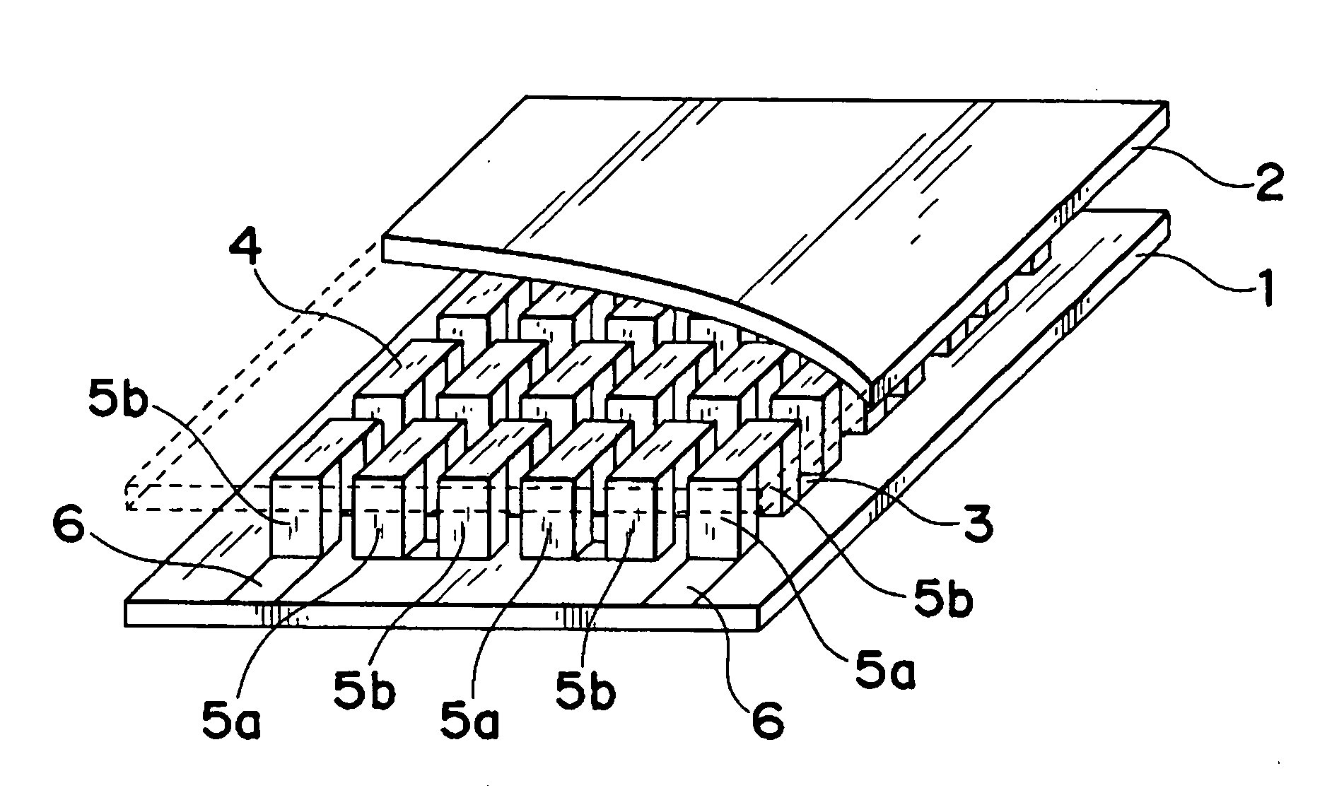
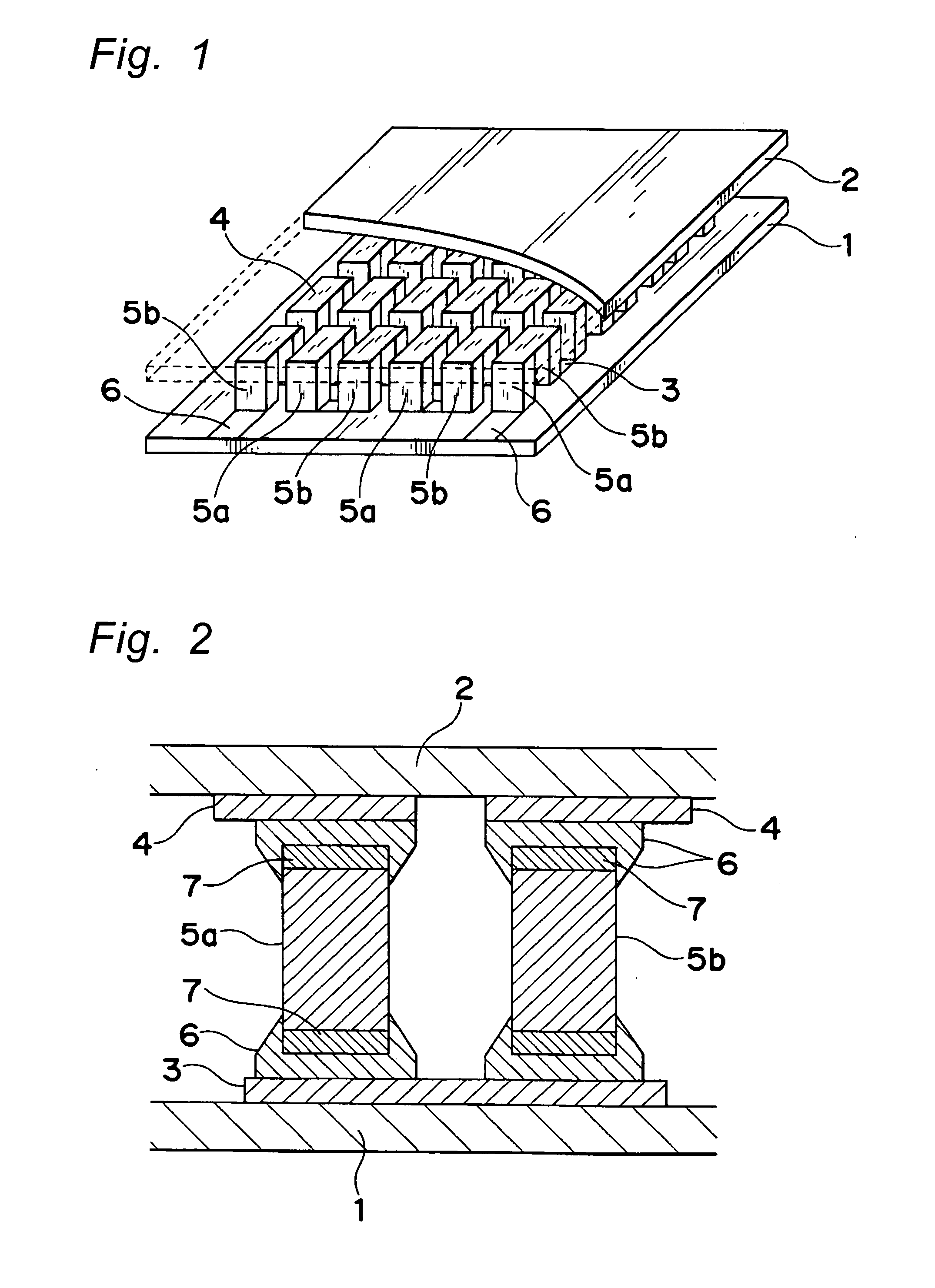
a technology of thermoelectric modules and thermoelectric materials, which is applied in the manufacture/treatment of thermoelectric devices, lighting and heating apparatuses, and the operation mode of machines. it can solve the problems of low cooling performance and efficiency, and the n-type thermoelectric material has a lower figure of merit, so as to prevent decomposition or quick growth of grains, reduce the quantity of carbon, and facilitate the effect of heat generation

Active Publication Date: 2007-05-03
KYOCERA CORP
View PDF5 Cites 51 Cited by
  • Summary
  • Abstract
  • Description
  • Claims
  • Application Information

AI Technical Summary

Benefits of technology

[0025] A second object of the present invention is to provide a directionally solidified thermoelectric crystalline material that has the figure of merit improved by decreasing the thermal conductivity and a method for manufacturing the same, a thermoelectric element and a thermoelectric module that has greatly improved cooling performance and cooling efficiency.
[0060] It is also preferable that molding pressure for forming the green compact is 10 MPa or higher. By setting the pressure to 10 MPa or higher, it is made possible to increase the sustaining force of the green compact, make the green compact easier to handle when manufacturing and proceed the sintering process effectively.

Problems solved by technology

The compositions and methods described in the documents cited above, however, there has been such a problem that the N type thermoelectric material has a lower figure of merit than that of the P type thermoelectric material.
Therefore, when the P-type and N-type thermoelectric crystalline material are used together to make a cooling element, the element has low cooling performance and low efficiency and cannot be readily applied to refrigerator for home use.
According to Japanese Unexamined Patent Publication (Kokai) No. 8-32588 and Japanese Unexamined Patent Publication (Kokai) No. 1-106478, however, values of the figure of merit of the thermoelectric materials made from these sintered materials are about 2.8×10⁻³ / K at the best, and the material can be used as a cooling element but has low levels of cooling performance and efficiency, thus restricting its applications and making it difficult to use in a refrigerator for home use.
As a result, means for improving the figure of merit are restricted to adjustment of the composition and optimization of the conditions of directional solidification which, even when carried out, can achieve an insignificant improvement in the figure of merit.
This limitation is partly due to the high thermal conductivity of the directionally solidified thermoelectric crystalline material.
Thus improvement of the figure of merit of the directionally solidified thermoelectric crystalline material of the prior art has been limited to about 3×10⁻³ / K due to high thermal conductivity.
Better mechanical properties than those of the melt-refined materials can be obtained by the use of the hot press process, although improvements of the characteristics are hampered by the oxidation of the stock material powder.
However, the thermoelectric material described in Japanese Unexamined Patent Publication (Kokai) No. 3-016281 has such a problem that heat treatment for removing fine particles is applied in the state of powder that has particle size in a range from 10 to 200 μm, and therefore the strength decreases.
There has also been such a problem that tendency of the powder to coagulate increases after the heat treatment which results in a longer time taken to insert the powder for sintering and the performance varies depending on the degree of coagulation, while the sintered material thus obtained has lower strength.
The method of manufacturing the thermoelectric material described in Japanese Unexamined Patent Publication (Kokai) No. 10-074984 has such a problem that, in addition to the necessity to sinter the powder, that has been subjected to heat treatment, under a pressure similarly to the case of patent document 2, it is not suited to mass production because the liquid quenching process that requires a special facility is employed, and the characteristic becomes unstable depending on the method of pressurized sintering, thus difference is likely to occur between the inside and the outside.
In the case of the method of manufacturing the thermoelectric material described in Japanese Unexamined Patent Publication (Kokai) No. 9-18060, since the stock material is prepared in a short period of time, quantity of oxygen in the material can be reduced, although a number of processes are involved and the processes are complicated, while performance cannot be improved sufficiently.
In the case of the method of manufacturing the thermoelectric material described in Japanese Unexamined Patent Publication (Kokai) No. 5-55640, since the powder is sintered while removing oxygen that has deposited on the surface of the particles of the stock material powder, though there is an effect of reducing the cost, it is difficult to achieve sufficient reduction of oxygen in the green compact and it is difficult to improve the performance, and the characteristic is unstable with difference likely to occur between the inside and the outside.
Thus with the methods of manufacturing the thermoelectric element of the prior art, the methods are simple but satisfactory performance cannot be achieved, or it has been difficult to obtain a thermoelectric material that has favorable property for mass production and high performance at the same time.
As described above, although the thermoelectric material is required to have the figure of merit greatly improved, thermoelectric materials of the prior art have low values of figure of merit and there have been limitation on expanding the applications of the thermoelectric element made by using the thermoelectric material and the thermoelectric module.
The thermoelectric materials of the prior art also have such a problem that tendency of the powder to coagulate increases after the heat treatment which results in a longer time taken to charge the powder for sintering and the performance varies depending on the degree of coagulation, while the sintered material thus obtained has a low strength.

Method used


Image

  • Thermoelectric material, thermoelectric element, thermoelectric module and methods for manufacturing the same
  • Thermoelectric material, thermoelectric element, thermoelectric module and methods for manufacturing the same

Examples


first embodiment

[0070] The first embodiment of the present invention relates to an N type thermoelectric material that contains bromine and iodine and a method for manufacturing the same, and a thermoelectric element obtained by processing the N type thermoelectric material.

[0071] It is important that the N type thermoelectric material of the first embodiment contains at least one kind of Bi and Sb and at least one kind of Te and Se as main components, and contains bromine (Br) and iodine (I) as dopant for adjusting the carrier concentration.

[0072] The most preferable composite known is (Bi2Te3)0.95(Bi2Se3)0.05 or (Bi2Te3)0.90(Sb2Te3)0.05(Sb2Se3)0.05 having 0.06 to 0.09% by weight of SbI3 added as a dopant.

[0073] The N type thermoelectric material of this type of composition, when at least two kinds selected from among Bi, Sb, Te and Se are contained as main components, makes a thermoelectric material that has high value of figure of merit near the room temperature. Adding Br and I together as t...

second embodiment

[0091] Now a second embodiment of the present invention will be described in detail.

[0092] The second embodiment relates to a directionally solidified thermoelectric crystalline material that contains a boron compound and a method for manufacturing the same, a thermoelectric element obtained by processing the thermoelectric crystalline material and thermoelectric module.

[0093] It is important that the directionally solidified thermoelectric crystalline material of the second embodiment is a thermoelectric crystalline material constituted from uniaxially oriented crystal that contains at least two elements selected from among Bi, Sb, Te and Se as main components, and contains a boron (B) compound.

[0094] The composition of the directionally solidified thermoelectric crystalline material can be made such that has high figure of merit at room temperature, by using at least two elements selected from among Bi, Sb, Te and Se as the main components. In addition, the figure of merit is i...

third embodiment

[0115] It is important that the thermoelectric material according to the third embodiment of the present invention is a dense material that contains at least two elements selected from among a group consisting of Bi, Sb, Te and Se. Such a material has a higher value of figure of merit, and is preferably A2B3 type intermetallic compound, for example a semiconductor crystal where A is substituted by Bi and / or Sb and B is substituted by Te and / or Se, and the ratio B / A is in a range from 1.4 to 1.6, which is preferable for improving the figure of merit at the room temperature.

[0116] As the A2B3 type intermetallic compound, at least one kind of Bi2Te3, Sb2Te3 and Bi2Se3, Bi2Te3-xSex, (x is from 0.05 to 0.25) that is a solid solution of Bi2Te3 and Bi2Se3, or BixSb2-xTe3, (x is from 0.1 to 0.6) that is a solid solution of Bi2Te3 and Sb2Te3 may be used.

[0117] An impurity may be added as a dopant to the intermetallic compound so as to turn it efficiently into a semiconductor. For example, ...


PUM

PropertyMeasurementUnit
lengthaaaaaaaaaa
particle sizeaaaaaaaaaa
temperatureaaaaaaaaaa

Abstract

T provide an N type thermoelectric material having figure of the merit improved to be comparable to or higher than that of P type thermoelectric material, the N type thermoelectric material of the present invention contains at least one kind of Bi and Sb and at least one kind of Te and Se as main components, and contains bromine (Br) and iodine (I) to have carrier in such a concentration that corresponds to the contents of bromine (Br) and iodine (I).

Description

TECHNICAL FIELD [0001] The present invention relates to a thermoelectric module used for cooling a heat generating device such as semiconductor and in various cooling devices, a thermoelectric element installed in the thermoelectric module, a thermoelectric material used in the thermoelectric element, and methods for manufacturing the same. BACKGROUND ART [0002] Thermoelectric modules, that utilize the Peltier effect to generate heat at one end thereof and absorbs heat from the environment on the other end when electric current flows therein, have been used in cooling applications. The thermoelectric module is envisioned to be particularly promising in such applications as temperature control for laser diode, portable refrigerator, thermostat, photo-detector device and semiconductor manufacturing apparatus. Recently, application of the thermoelectric module to refrigerator and air conditioner for home use is studied vigorously, because of such advantages as the capability to operate...

Claims


Application Information

Patent Timeline
Patent Type & Authority Applications(United States)
IPC IPC(8): H01L35/16H01L35/20B22F3/24F25B21/02C22C1/04C22C12/00H01L23/38H01L35/34
CPCC22C12/00H01L23/38H01L35/16H01L35/34H01L2924/0002H01L2924/00H10N10/852H10N10/01
Inventor TAJIMA, KENICHI
Owner KYOCERA CORP
Learn More