Wave soldering fixture

a soldering fixture and wave technology, applied in the direction of soldering apparatus, manufacturing tools, auxillary welding devices, etc., can solve the problems of board bowing, limited supply of components, etc., to achieve the effect of improving the efficiency of production and maintenance, and simplifying the problem of maintaining registration

Inactive Publication Date: 2001-05-29
CHUNG HENRY
View PDF5 Cites 86 Cited by
  • Summary
  • Abstract
  • Description
  • Claims
  • Application Information

AI Technical Summary

Problems solved by technology

The problem with this technique was that the trailing and leading sides of the PCB had no support, thus causing the middle of the board to bow in the middle from the front to the back.
With the demand for greater density of components (IC's), exposure of the PCB to the heat of a solder wave at 450.degree. F. became a more important issue.
All of these techniques, used separately or in combination, present limitations to the continued demand for greater component density and economy of manufacture.
Even with accurate machining of the poc

Method used


Image

  • Wave soldering fixture
  • Wave soldering fixture
  • Wave soldering fixture

Examples


Embodiment Construction

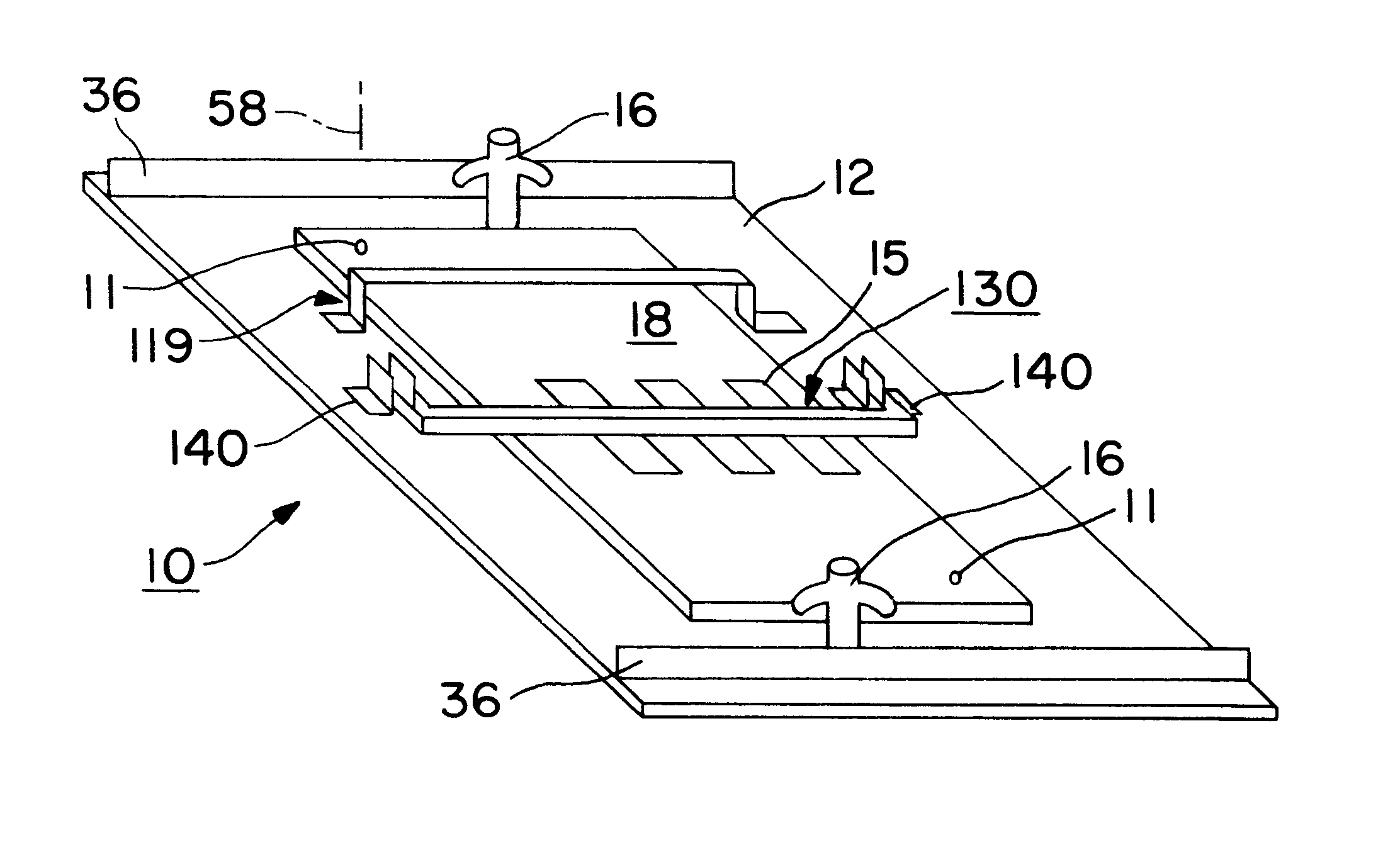
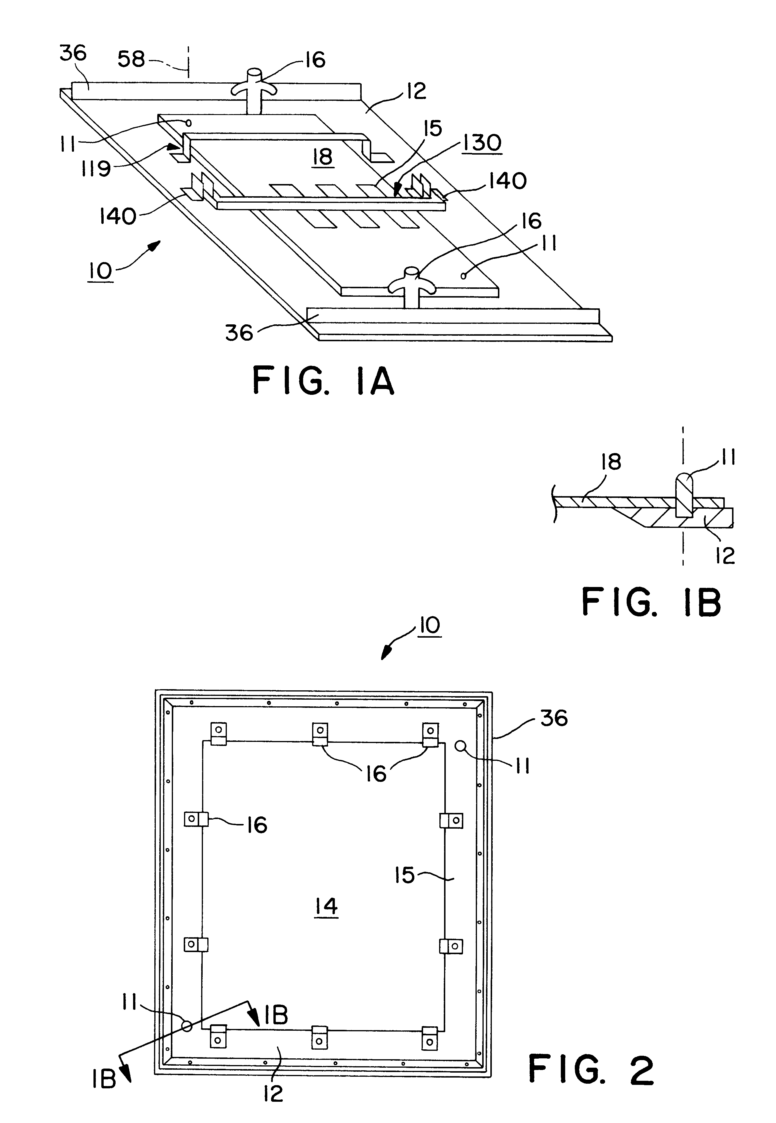
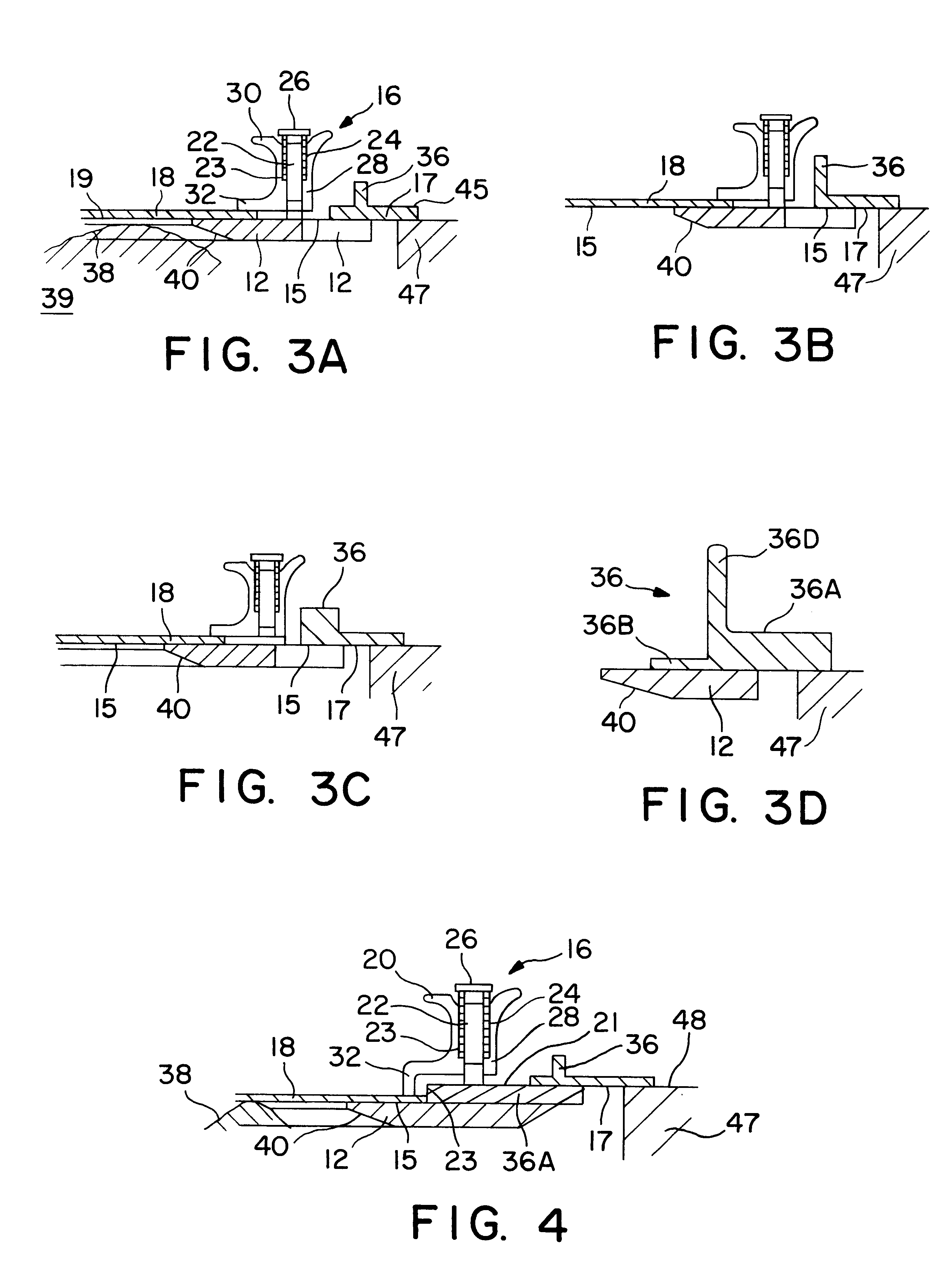
Turning now to a discussion of the drawings, FIG. 1 shows the fixture 10 of this invention which satisfies the objects outlined in the SUMMARY. There are shown a PCB 18 mounted onto a frame 12, a plurality of hold down clamps 16 (two are shown in FIG. 1), stiffeners 36, a board support bar 114, and a hold down bar 130. As shown in detail in FIG. 1B, pair of locating pins 11 in frame 12 pass through the PCB 18 and maintain registration of the PCB 18 with the opening in the frame. 12. Details of the stiffener 36 (FIGS. 2A,B) , hold down bar 130 (FIGS. 6A-C, 7), and board support bar 114 (FIGS. 5A-D) are discussed in following paragraphs

FIG. 2 shows is a plan view of the clamps and stiffeners of this invention. The fixture 10 includes a frame 12 having a rectangular frame opening 14. A plurality of spring loaded clamps 16 (ten are shown in FIG. 2) are mounted on a frame reference surface 15 of the frame 12 for detachably holding the PCB 18 on the frame reference surface 15. Details of ...


PUM

PropertyMeasurementUnit
Angleaaaaaaaaaa
Currentaaaaaaaaaa
Currentaaaaaaaaaa

Abstract

An apparatus used in a process for supporting a printed circuit board during a wave soldering operation including a frame with a frame opening in which a surface of the frame supports the board and also serves as a reference surface for vertically positioning the board above the solder pool. The board is secured against the reference surface with spring loaded clamps. Stiffeners preferably being an aluminum extrusion having a Tee or angle cross section is mounted along the outside edge of the reference surface of the frame and has a second reference surface facing in a direction opposite the reference surface of the frame. The second reference surface on the extrusion is accessible for support by a slide rail so that the height of the reference surface of the frame above the surface of the pool is independent of the thickness of the board or frame. A board support bar for minimizing warpage of the board from heat is disclosed as well as a hold down bar that secures components on the board so that they do not float away when contacted by the solder wave.

Description

This invention relates to apparatus for assembling components on printed circuit boards PCBs and particularly to a fixture that supports the PCB through a wave soldering step. In the context of this specification and in accordance with the practices of the art, the terms, pallet, fixture, carrier and rack will be understood to have a common meaning.BACKGROUND AND INFORMATION DISCLOSUREThe technology for manufacturing circuits comprising components mounted on boards has evolved continuously during the past fifty years keeping pace with the evolution of discrete semiconductor devices to present high density integrated circuits on a chip.In the earliest techniques for the manufacture of PCBs, components were hand soldered onto the board. The next evolutionary step involved exposing the unsupported PCB to a solder wave. The problem with this technique was that the trailing and leading sides of the PCB had no support, thus causing the middle of the board to bow in the middle from the fro...

Claims


Application Information

Patent Timeline
IPC IPC(8): B23K3/08B23K3/00
CPCB23K3/087B23K2201/42B23K2101/42
Inventor CHUNG, HENRY
Owner CHUNG HENRY
Why Eureka
Try Eureka