Compensating layer to reduce wavefront errors in coatings on mirrors for optical systems

a technology of optical systems and compensating layers, applied in the field of optical systems, can solve the problems of difficult to provide adequate spacing between layers, difficult to achieve uniform deposition of multi-layer coatings on large optical components such as reflecting mirrors, and wavefront errors in optical beams reflected from reflecting surfaces, etc., to reduce or eliminate wavefront errors, reduce wavefront errors, and reduce wavefront errors

Inactive Publication Date: 2001-07-03
THE BF GOODRICH CO
View PDF7 Cites 8 Cited by
  • Summary
  • Abstract
  • Description
  • Claims
  • Application Information

AI Technical Summary

Benefits of technology

Accordingly, a principal object of this invention is to provide a method for designing and manufacturing an optical coating that will reduce or eliminate the wavefront error due to variations in the thickness of an optical coating on an optical surface, for example a mirror.
Another object to this invention is to produce a method which will reduce wavefront error due to variations in thickness of an optical coating when a multi-layer coating is used.
A third object of this invention is to produce a method for reducing wavefront error due to the variation in thickness of an optical coating when a coating is deposited on a reflecting optical surface having a large surface area.
The above objectives and other advantages of the invention are achieved by using a compensating layer which is applied over the top layer of a reflection coating applied to an optical surface. The compensating layer compensates for variations in thickness of the reflection coating applied to the optical element to reduce phase errors due to variations in the thicknesses of the applied layers at different points across the reflecting surface of the optical element, thereby reducing the wavefront error introduced into the reflected signal due to non-uniformities present in the reflection coating.

Problems solved by technology

It is also known that thickness variations in the coating across the surface of an optical element will cause wavefront errors in the optical beam reflected from the reflecting surface.
It is well known and is a common problem in the field of depositing coatings that the uniform deposition of a multi-layer coating is difficult to achieve on a large optical component such as a reflecting mirror, due to the physical constraints of the coating chambers utilized for depositing optical coatings.
In particular, it is often difficult to provide adequate spacing between the source of the material to be deposited and the surface to be coated to avoid the non-uniform deposition of material onto the surface to be coated.
While various techniques, such as rotation of the optical element to be coated and the use of masks, can be used to reduce the non-uniformity, it is difficult to entirely eliminate the wavefront error due to the variation in thickness of the deposited coating.
If the coating on the mirror's surface is non-uniform in thickness, the phase shift in one region of the mirror, for example at the location where the coating is thin, will not match the phase shift elsewhere, thereby causing a wavefront error in the reflected beam.
The wavefront error has only been a minor problem for most optical components, and thus this problem has received little study.

Method used


Image

  • Compensating layer to reduce wavefront errors in coatings on mirrors for optical systems
  • Compensating layer to reduce wavefront errors in coatings on mirrors for optical systems
  • Compensating layer to reduce wavefront errors in coatings on mirrors for optical systems

Examples


Embodiment Construction

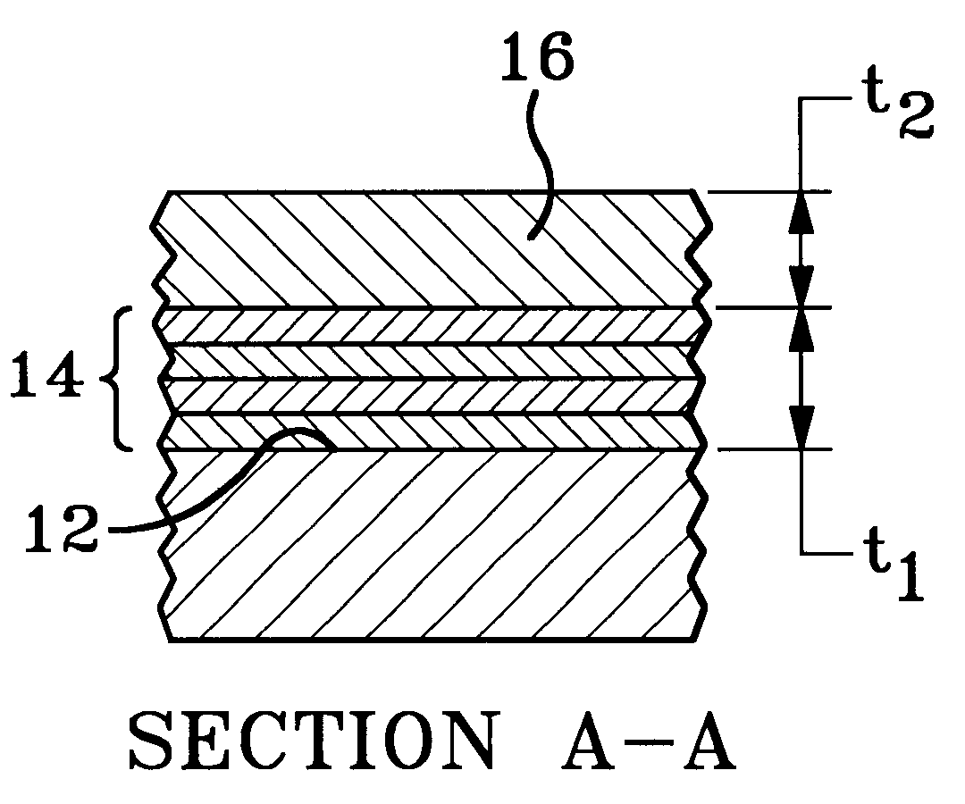
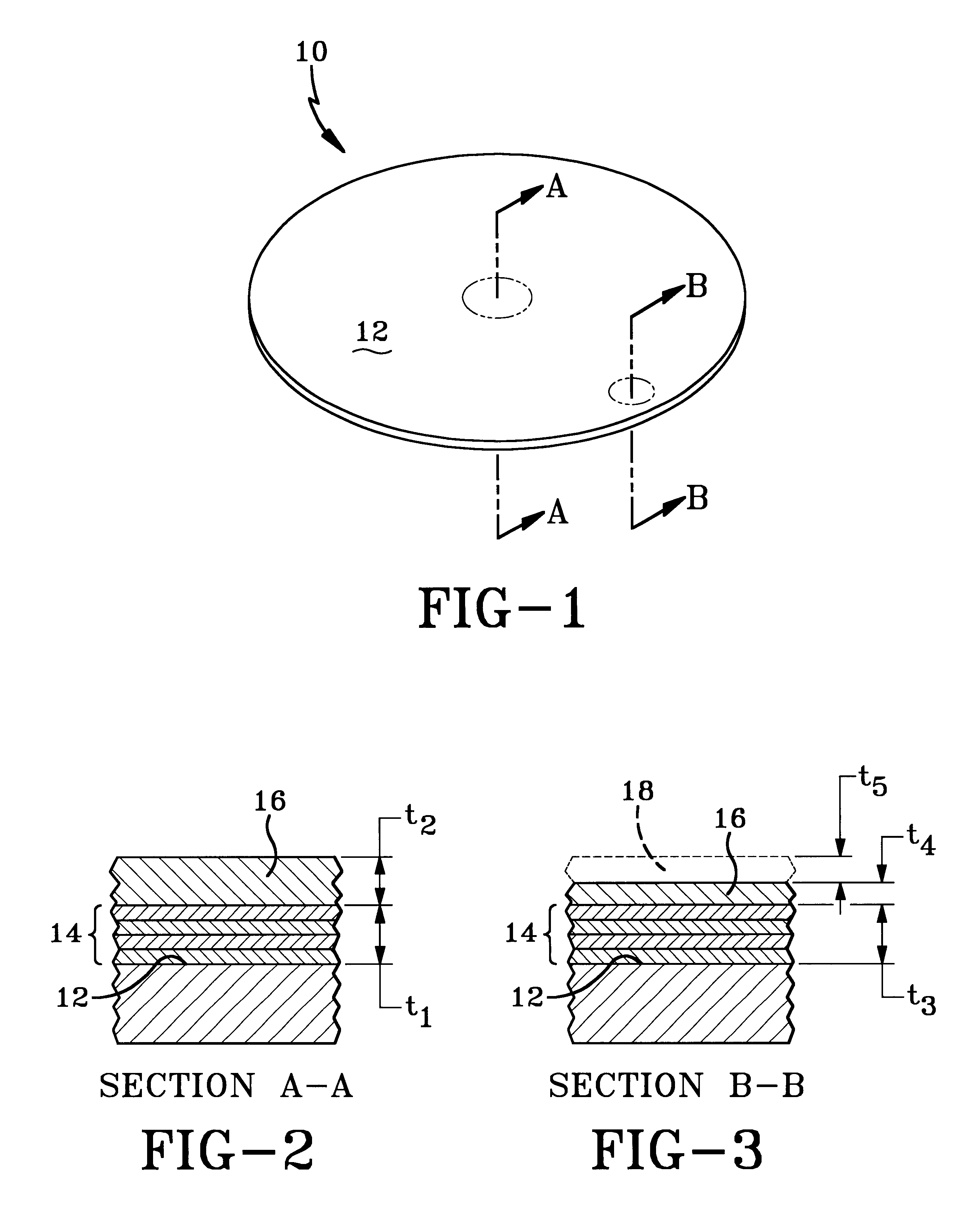
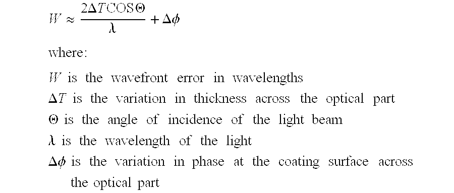
Referring to the drawing, FIG. 1 shows a reflecting mirror 10 having a reflecting coating composed of layers 14 and 16. These layers were deposited on the substrate surface 12. For example, the coating 14 may consist of a twenty-one layer coating composed of quarter-wave optical thickness alternating layers of titanium dioxide and silicon dioxide. The alternating layers of the reflection coating are deposited in a manner well known in the art, for example by electron beam deposition or by sputtering. It will be appreciated by those skilled in the art that due to the geometry of the coating chambers used for depositing materials on optical elements, such as reflecting coating of the foregoing design, non-uniformities in coating thickness can occur across the surface of the coated optical element, for example across the surface of the mirror 10. Thus, the thickness of each layer at location B is slightly different than the thickness at location A. Principally, such errors are due to t...


PUM

PropertyMeasurementUnit
thicknessaaaaaaaaaa
thicknessaaaaaaaaaa
wavelengthaaaaaaaaaa

Abstract

A method is disclosed for reducing or eliminating the wavefront error caused by variations in the thickness of an optical coating applied to a mirror without requiring that the thickness variation in the optical coating be reduced to reduce the wavefront error. The reduction in the wavefront error is achieved by adding a compensating layer to the top of the optical coating. The thickness of the compensating layer is directly proportional to the thickness of the optical coating and inversely proportional to one minus the index of refraction of the material used for the compensating layer.

Description

1. Field of the InventionThis invention relates to optical systems in general and, in particular, to optical systems having reflecting elements containing multi-layer coatings on the reflecting surface.2. Summary of the Prior ArtThe use of multi-layer coatings to increase the reflectance of the front of an optical surface, for example a mirror, is well known in the art. Multi-layer reflection coatings are applied by alternately depositing layers of material, such as silicon dioxide and titanium dioxide, in alternating layers in thicknesses calculated by methods well known to those skilled in the art, to increase the reflectance of a reflecting surface at desired wavelengths. Many known techniques are available for depositing the multi-layer coatings. For example, they may be deposited in a coating chamber by sputtering or by electron beam deposition. It is also known that thickness variations in the coating across the surface of an optical element will cause wavefront errors in the ...

Claims


Application Information

Patent Timeline
Patent Type & Authority Patents(United States)
IPC IPC(8): G02B1/10G02B27/00G02B5/08
CPCG02B1/10G02B27/0025G02B5/08Y10S359/90G02B1/11
Inventor DAVIS, WILLIAM J.
Owner THE BF GOODRICH CO
Why Eureka
Try Eureka