In-plane field type liquid crystal display device comprising liquid crystal molecules with more than two kinds of reorientation directions
- Summary
- Abstract
- Description
- Claims
- Application Information
AI Technical Summary
Problems solved by technology
Method used
Image
Examples
example 2
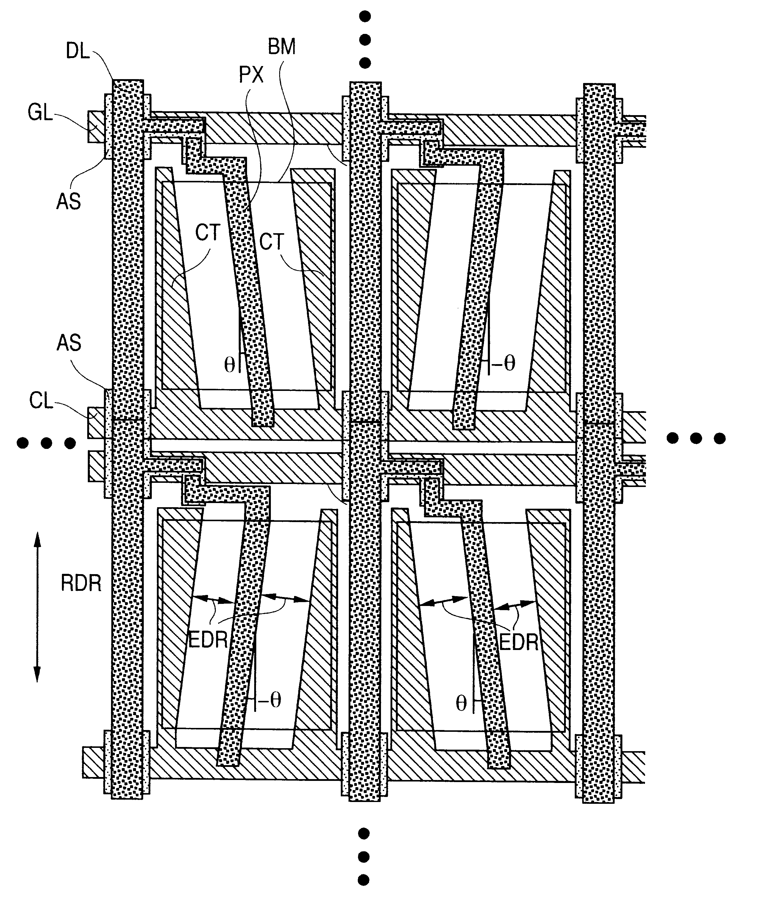
FIG. 19 is an illustration showing another example of this embodiment in the unit picture element.
The liquid crystal display device is manufactured similarly to example 1 except that shapes of two pixel electrode and three counter electrodes are changed as shown in FIG. 19 and the gap distance between pixel electrodes and counter electrodes is changed to 15 .mu.m.
As the result of measuring viewing angle characteristics similarly to the case of exmple 1, no tone reversal occurred at any angle within .+-.60.degree. of .phi..
example 3
The liquid crystal display device is manufactured similarly to example 2 except that angles of the bent portions of pixel electrodes and counter electrodes are changed to 178.degree..
As the result of measuring viewing angle characteristics similarly to the case of example 1, no tone reversal occurred at any angle within .+-.60.degree. of .phi..
As the result of measuring a voltage at which the transmittance is maximized and a voltage at which the transmittance is equal to 1% of the maximum transmittance, voltages of 2.5 V and 1.5 V are obtained respectively. The difference between the voltages is 1.0 V, which is remarkably small.
example 4
FIG. 20 is an illustration showing example 4 of this embodiment in one picture element.
The liquid crystal display device is manufactured similarly to example 3 except that two types of gap distances of 20 .mu.m and 10 .mu.m are formed between pixel electrodes and counter electrodes in one picture element.
As the result of measuring viewing angle characteristics similarly to example 1, no tone reversal occurred at any angle within .+-.60.degree. of .phi..
As the result of measuring a voltage at which the transmittance is maximized and a voltage at which the transmittance is equal to 1% of the maximum transmittance, voltages of 3.4 V and 1.0 V are obtained, respectively. The difference between the voltages is 2.4 V, which is large and suitable for displaying multiple gradation levels.
PUM
 Abstract
Description
Claims
Application Information


