Stepper with exposure time monitor

a stepper and monitor technology, applied in the field of semiconductor processing, can solve problems such as distorted patterns, misplaced patterns, and other defects, and change the functioning of electrical circuits

Inactive Publication Date: 2001-07-24
GLOBALFOUNDRIES INC
View PDF4 Cites 14 Cited by
  • Summary
  • Abstract
  • Description
  • Claims
  • Application Information

AI Technical Summary

Problems solved by technology

Errors in the photolithography process can cause a whole host of problems including, but not limited to, distorted patterns, misplaced patterns, and other defects.
These types of errors can ultimately result in undesirable changes in the functioning of the electrical circuits so that the wafer has to be scrapped.
Photolithography processes are performed at very small dimensions, so that they are also highly susceptible to contamination by unwanted variations in processing conditions.
There comes a point in the stepper exposure time automatic control process where the exposure time is inc

Method used


Image

  • Stepper with exposure time monitor
  • Stepper with exposure time monitor
  • Stepper with exposure time monitor

Examples


Embodiment Construction

Illustrative embodiments of the invention are described below. In the interest of clarity, not all features of an actual implementation are described in this specification. It will of course be appreciated that in the development of any such actual embodiment, numerous implementation-specific decisions must be made to achieve the developers'specific goals, such as compliance with system-related and business-related constraints, which will vary from one implementation to another. Moreover, it will be appreciated that such a development effort might be complex and time-consuming, but would nevertheless be a routine undertaking for those of ordinary skill in the art having the benefit of this disclosure.

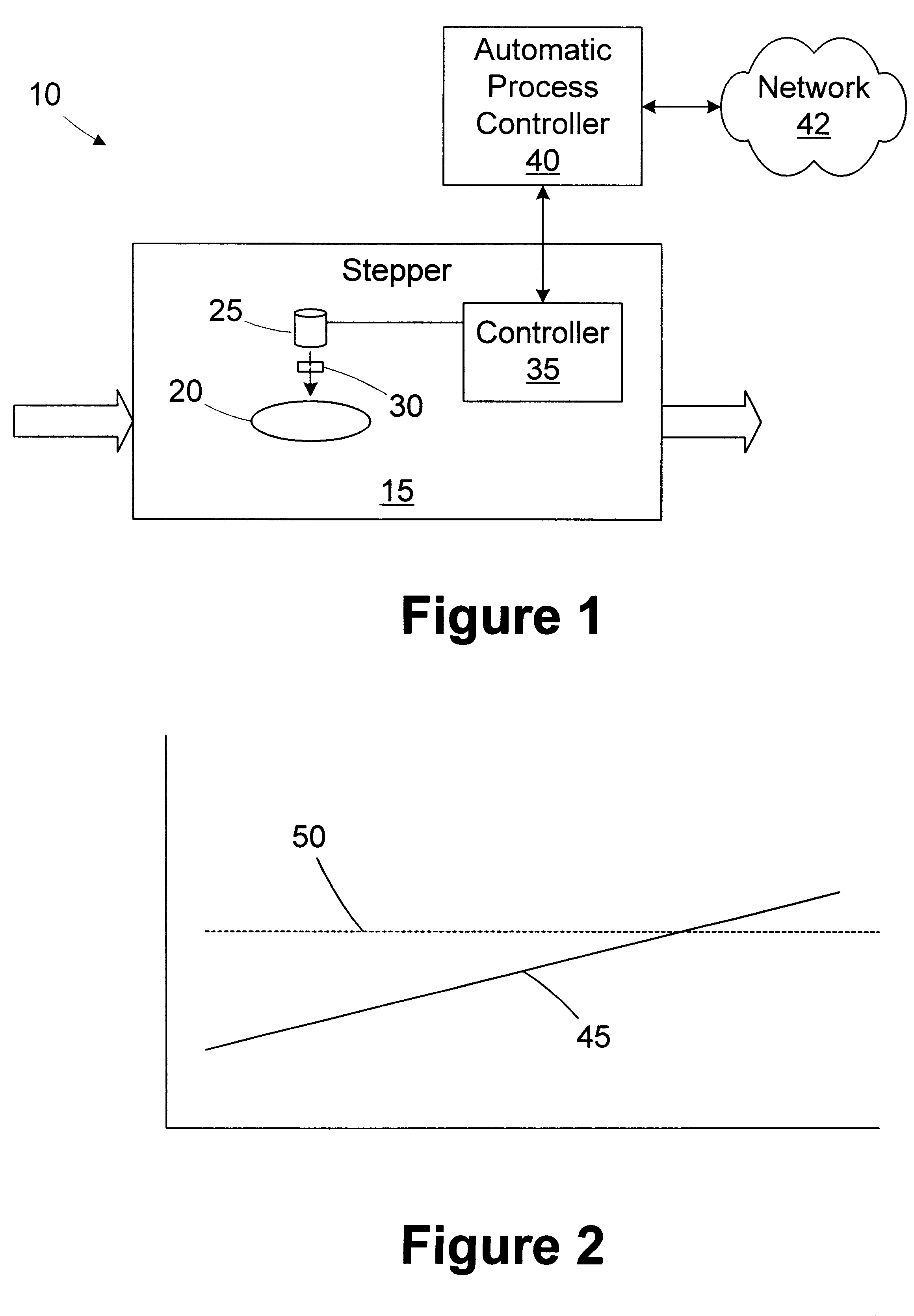
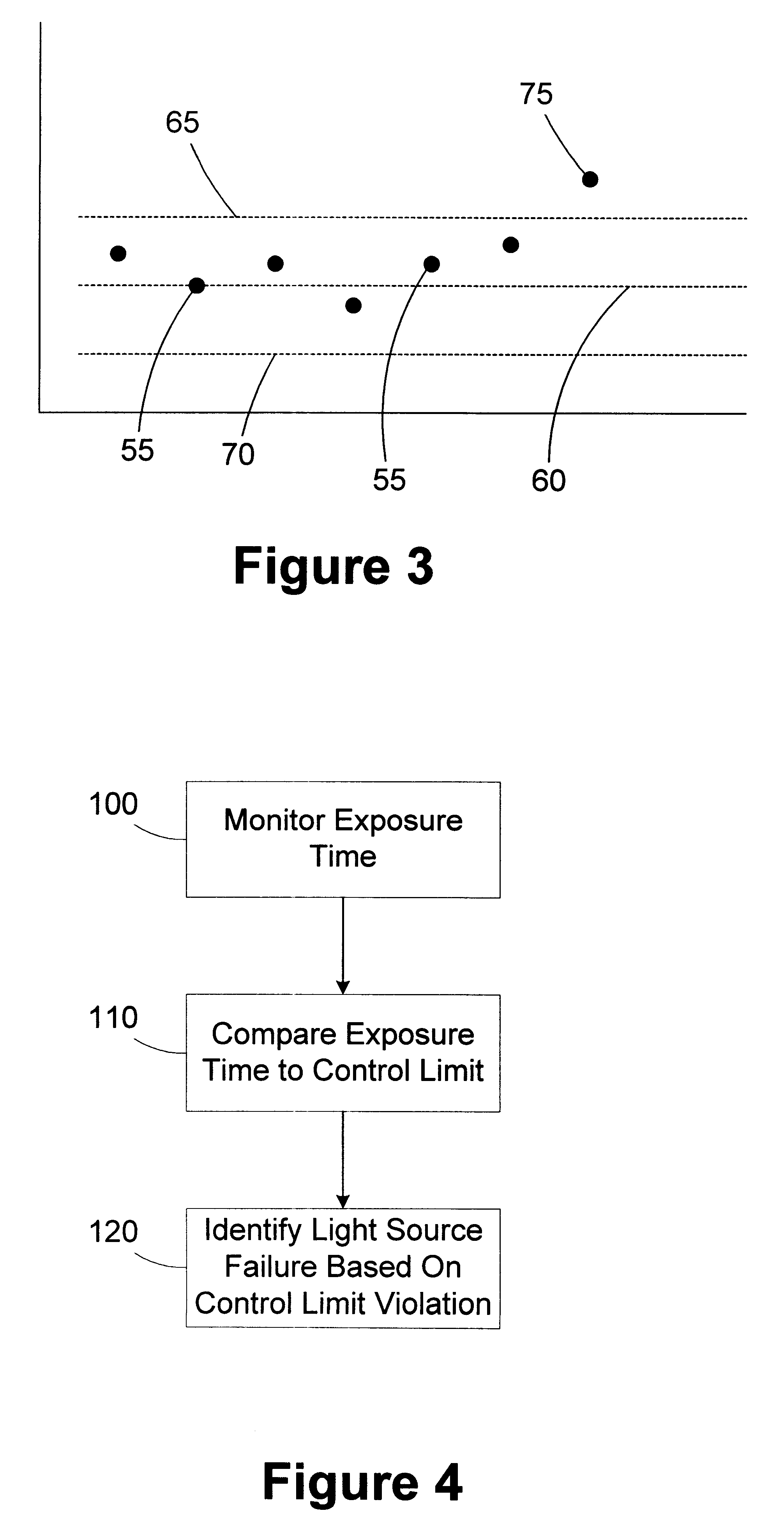
Referring to FIG. 1, a simplified block diagram of a processing tool 10 is provided. The processing tool 10 includes a stepper 15 used in a photolithography process for exposing a wafer 20 to a light source 25. The incident radiation from the light source 25 passes through a photomask 3...


PUM


Abstract

A method for detecting a degraded light source is provided. An exposure time associated with the light source is monitored. The exposure time is compared to at least one control limit. A degraded condition is identified based on the exposure time violating the control limit. A processing tool includes a stepper and an automatic process controller. The stepper has a light source and is adapted to illuminate a wafer for an exposure time. The automatic process controller is adapted to monitor the exposure time, compare the exposure time to at least one control limit, and identify a degraded condition based on the exposure time violating the control limit.

Description

1. Field of the InventionThis invention relates generally to semiconductor processing, and more particularly, to a stepper having a exposure time monitor for identifying a degraded lamp condition.2. Description of the Related ArtSemiconductor devices, or microchips, are manufactured from wafers of a substrate material. Layers of materials are added, removed, and / or treated during fabrication to create the electrical circuits that make up the device. The fabrication essentially comprises four basic operations. The four operations are:layering, or adding thin layers of various materials to a wafer from which a semiconductor is produced;patterning, or removing selected portions of added layers;doping, or placing specific amounts of dopants in the wafer surface through openings in the added layers; andheat treatment, or heating and cooling the materials to produce desired effects in the processed wafer.Although there are only four basic operations, they can be combined in hundreds of di...

Claims


Application Information

Patent Timeline
IPC IPC(8): G03F7/20
CPCG03F7/70525G03F7/70008
Inventor STEWART, EDWARD C.DOSS, CURTIS W.EDWARDS, RICHARD D.
Owner GLOBALFOUNDRIES INC
Why Eureka
Try Eureka