Refresh-type memory with zero write recovery time and no maximum cycle time

a memory and write recovery technology, applied in the field of memory devices and methods of semiconductor devices, can solve problems such as data errors, inability to hold data indefinitely, and inability to dram

Inactive Publication Date: 2001-08-14
SAMSUNG ELECTRONICS CO LTD
View PDF4 Cites 51 Cited by
  • Summary
  • Abstract
  • Description
  • Claims
  • Application Information

AI Technical Summary

Problems solved by technology

Because all capacitors exhibit charge leakage, a characteristic of the DRAM cell is that it cannot hold data indefinitely.
A charged storage node will eventually discharge to a point where it will be misread as a discharged storage node, causing a data error.
Whereas an SRAM can complete a write operation upon sensing the rising edge of the WE# pulse, this DRAM cannot.
As illustrated in FIG. 3, the op

Method used


Image

  • Refresh-type memory with zero write recovery time and no maximum cycle time
  • Refresh-type memory with zero write recovery time and no maximum cycle time
  • Refresh-type memory with zero write recovery time and no maximum cycle time

Examples


Embodiment Construction

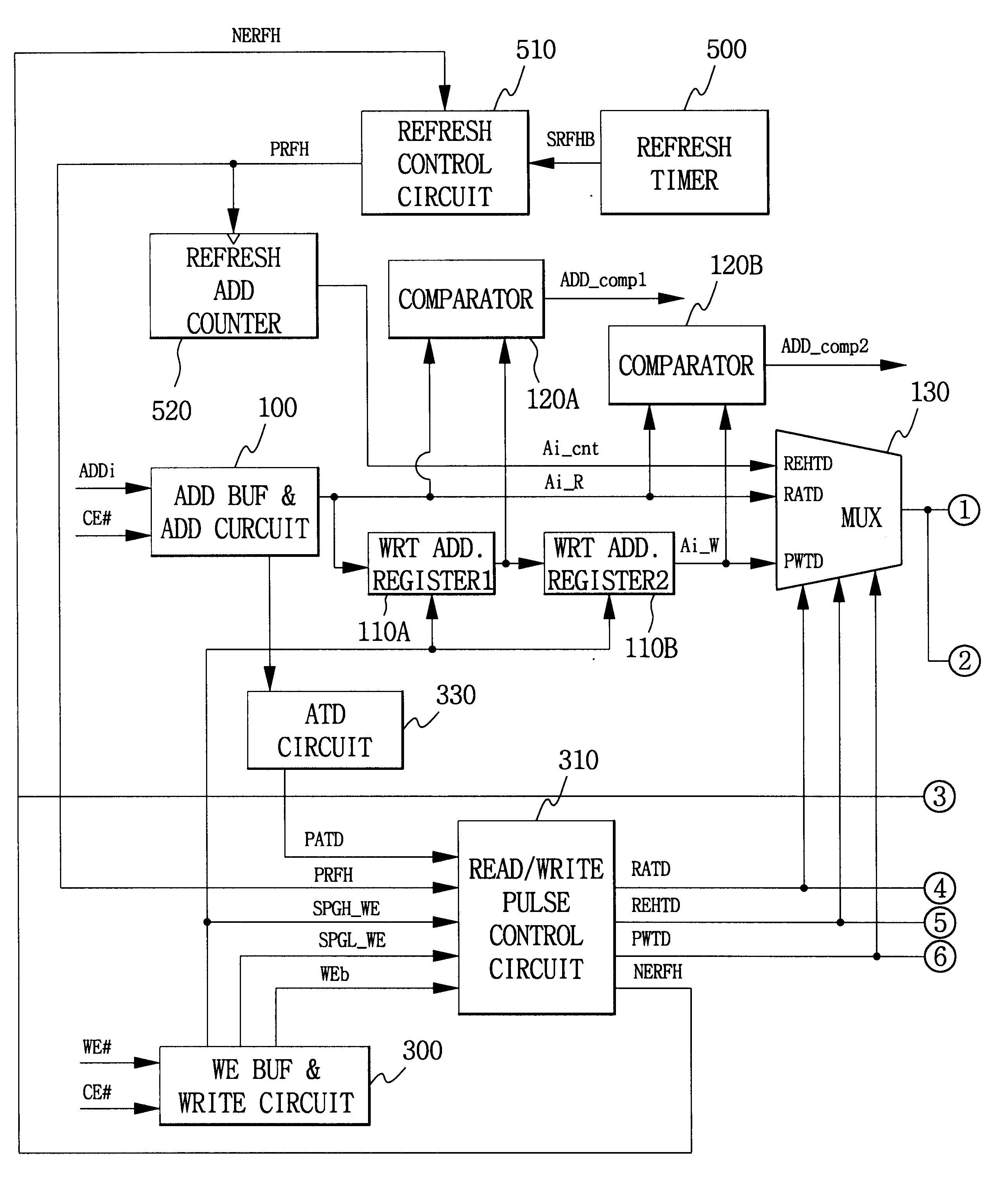
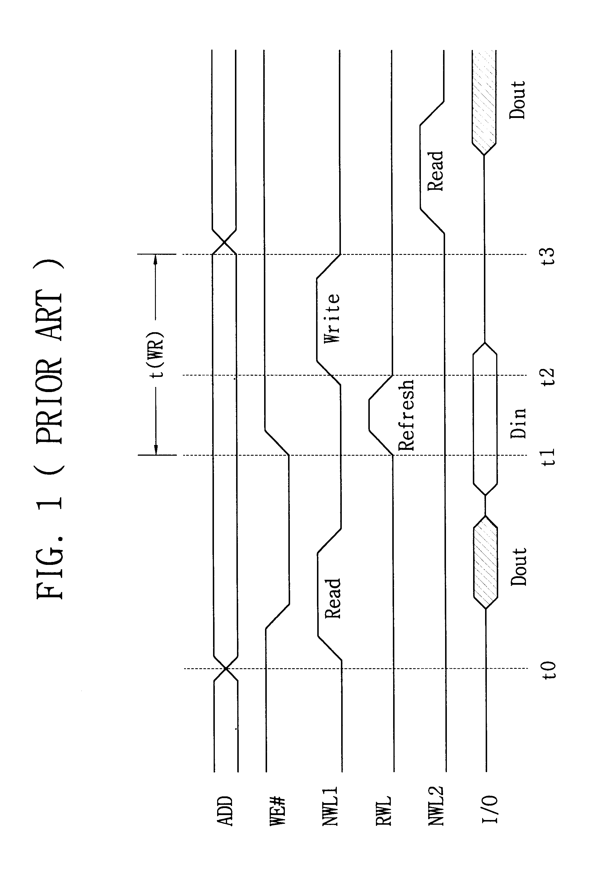
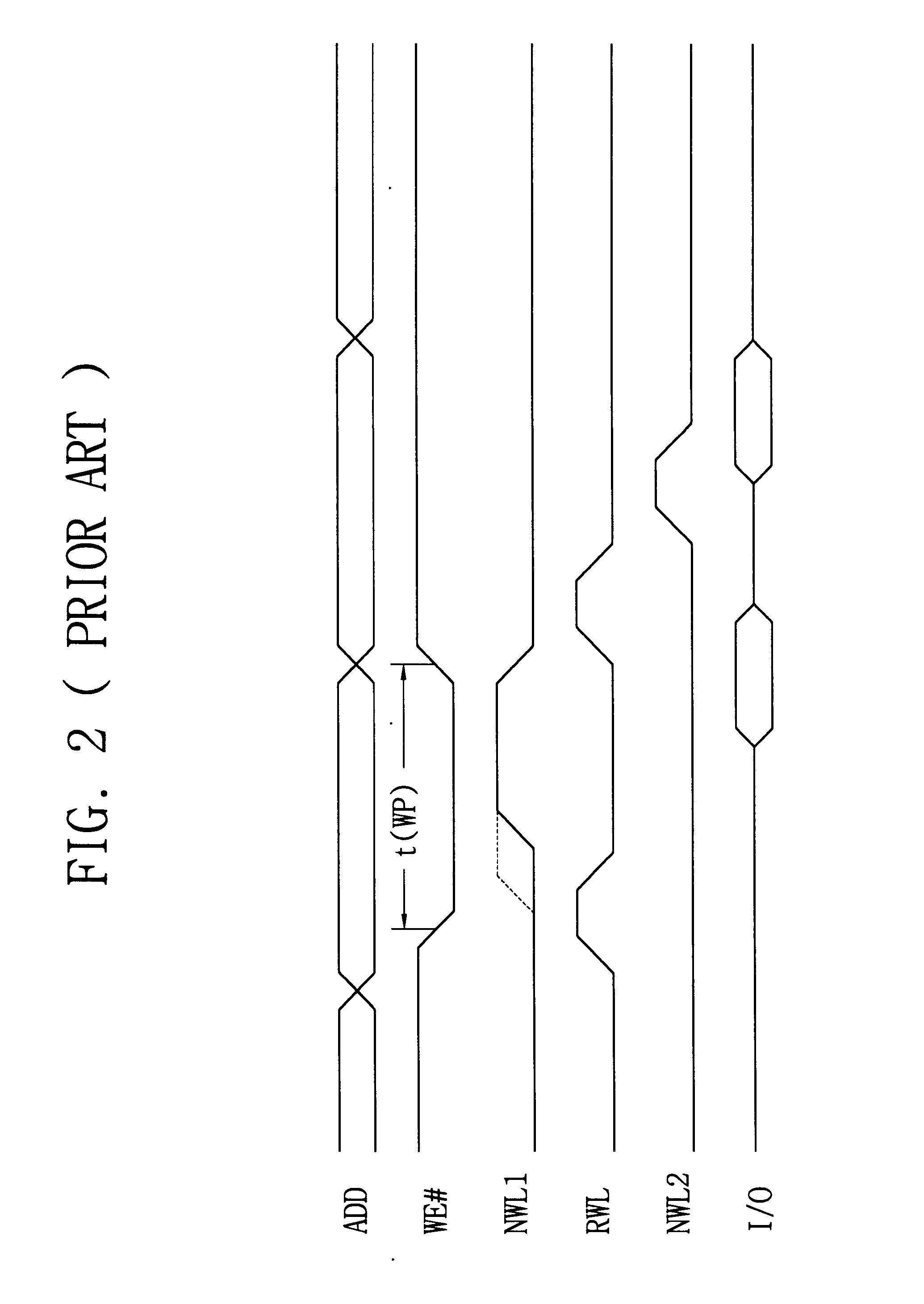
In the following description, several terms have defined meanings. A pulsed operation, such as a pulsed read or a pulsed write, refers to an operation that is internally sequenced, as opposed to an operation that begins and ends based upon transitions of an external signal. For example, a pulsed write operation may begin based upon an internal or external start signal, but the operation then proceeds according to internally-generated signals.

A late write refers to an internal pulsed write operation to the memory cell array. The distinguishing feature of a late write is that array address setup and data writing occur at some time after the external write operation during which the address and data were supplied to the device, with the external write address and data stored in temporary registers in the interim. The late write may occur, e.g., during a following external write operation. Another feature of a late write is the possibility that a request to read the data may occur befor...


PUM


Abstract

A semiconductor memory device and method for its operation are disclosed. The memory device uses refresh-type memory cells, but operates within the same timing parameters as a SRAM. A refreshing operation and a successful read/write operation can both be performed in a read/write cycle, with zero write recovery time. But if the read/write cycle goes long, multiple refreshing operations can also be performed during the read/write cycle. Thus the device operates with no maximum write cycle time limitation. In the disclosed method, an external write command causes the device to store the write address and data to registers instead of to the memory cell array. When the external write command signals that data is present, zero write recovery time is needed, since the registers require no address setup time. Because the memory cell array is not involved in this transaction, refresh operations can proceed as needed during the external write command, no matter how long the external write takes to complete. At a convenient time after the end of the external write command (e.g., during the next external write command), a short pulsed write operation transfers the data to the memory cell array.

Description

1. Field of the InventionThe present invention relates to a semiconductor memory device and method of operation, and more particularly, to a semiconductor memory device and method of operation wherein memory cells require refreshing of storage data, wherein refreshing operations are performed internally, and wherein the device operates externally with timing requirements similar to those of a static RAM.2. Description of the Related ArtRandom-access memory (RAM) devices store electronic data in an array of individually-addressable elements known as memory cells. Two basic types of RAM cells are prevalent in the market--the static RAM (SRAM) cell and the dynamic RAM (DRAM) cell. The SRAM cell has a static latching structure (e.g., comprising six transistors, or four transistors and two registers) that can store data indefinitely. The DRAM cell has a storage node (e.g., a capacitor) and a single access transistor. Data is stored in the cell by setting the charge state of the storage n...

Claims


Application Information

Patent Timeline
IPC IPC(8): G11C11/406G11C11/403G11C11/408G11C11/409
CPCG11C11/40615G11C11/406
Inventor KIM, CHANG-RAEPARK, JONG-YULCHUNG, MIN-CHULHAN, SANG-JIB
Owner SAMSUNG ELECTRONICS CO LTD
Why Eureka
Try Eureka