High speed buffer circuit with improved noise immunity

a buffer circuit and high-speed technology, applied in the field of buffer circuits, can solve the problems of slow low to high transition at the output terminal q1, m11 to rapidly weaken, and slow low to high transition at the output terminal q1

Inactive Publication Date: 2001-10-23
INTEGRATED DEVICE TECH INC
View PDF15 Cites 30 Cited by
  • Summary
  • Abstract
  • Description
  • Claims
  • Application Information

AI Technical Summary

Problems solved by technology

One disadvantage of circuit 5 is slow low to high transition at the output terminal Q1.
However, as the output terminal Q1 rises, the voltage across both the gate to source and drain to source reduce, causing M11 to rapidly become weak.
However, this circuit suffers from the following two disadvantages: 1) a high to low transition is slower since the transition is made from full Vcc as opposed to Vcc minus VT, and 2) more noise is generated on Vss since a greater amount of charge is discharged into Vss during the high to low transition.

Method used


Image

  • High speed buffer circuit with improved noise immunity
  • High speed buffer circuit with improved noise immunity
  • High speed buffer circuit with improved noise immunity

Examples


Embodiment Construction

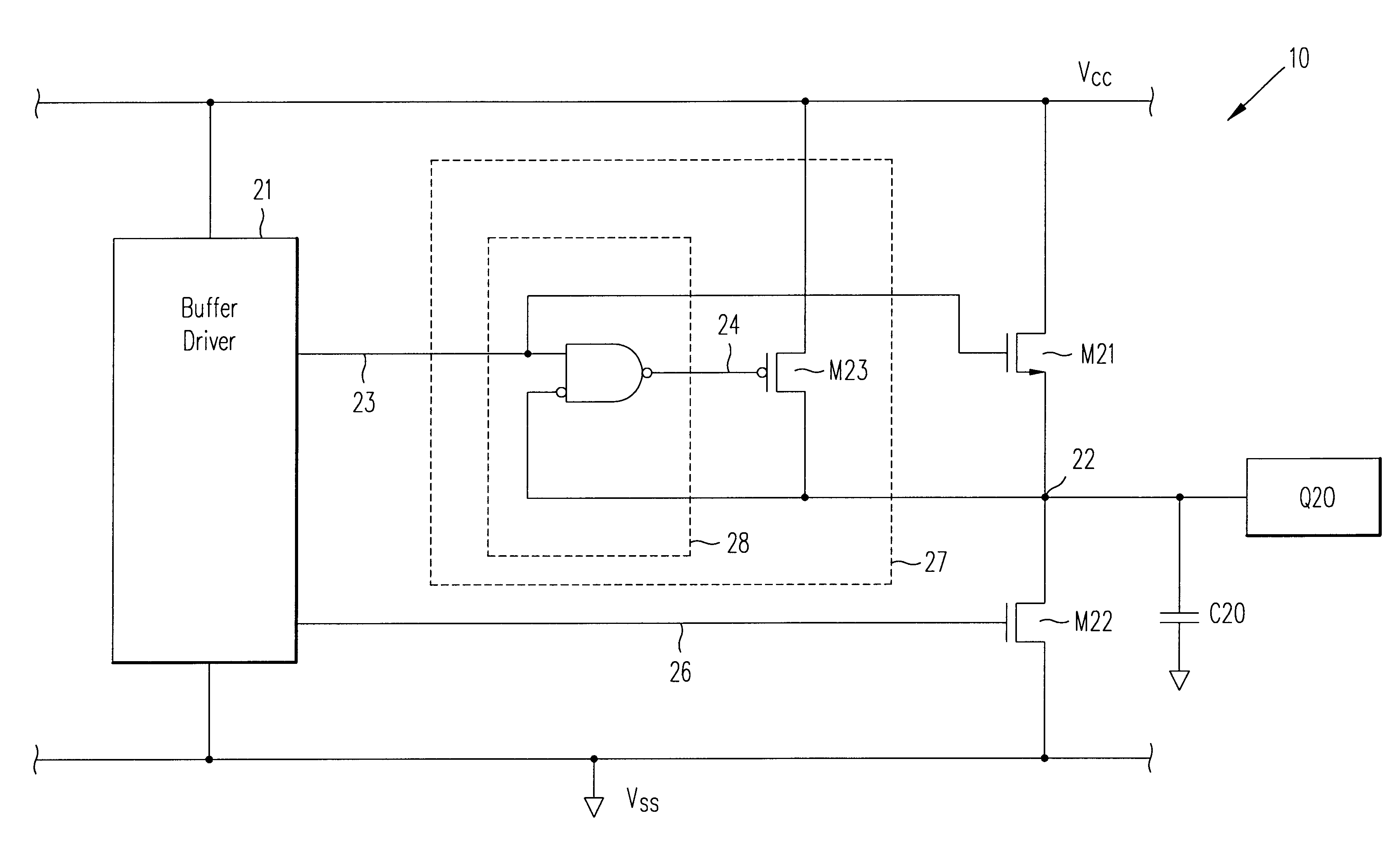
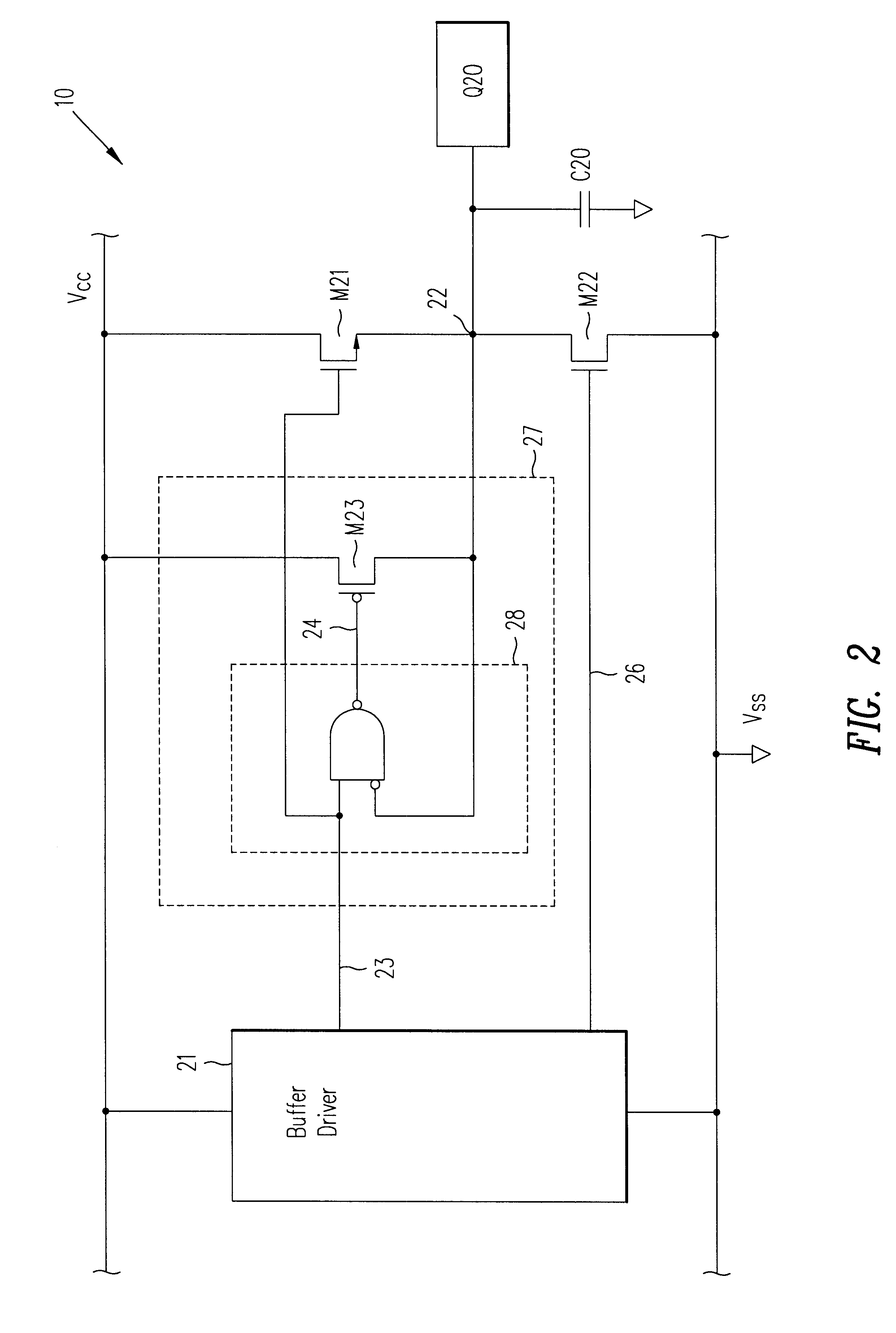
Circuit 25 in FIG. 2 is one embodiment of the present invention. Circuit 25 includes all the elements of prior art circuit 5 (FIG. 1A) plus the feedback circuit 27. Feedback circuit 27 comprises a logic gate 28 and a PMOS transistor M23. Logic gate 28 is a two input NAND gate having an inverted input. The inverted input is connected to the output terminal Q20 (at node 22), and the non-inverted input of logic gate 28 is connected to the buffer driver 21 at lead 23. The output terminal of logic gate 28 is connected to the gate of transistor M23 at lead 24. The PMOS transistor M23 has its source connected to Vcc, its gate connected to lead 24 and its drain connected to the output terminal Q20. NMOS transistor M21 has its drain connected to Vcc, its gate connected to the buffer driver 21 at lead 23, and its source connected to the output terminal Q20. NMOS transistor M22 has its drain connected to the output terminal Q20, its gate connected to the buffer driver 21 at lead 26, and its so...


PUM


Abstract

In a buffer circuit a pull-up circuit causes an output terminal of the buffer circuit make a transition from a low voltage to a high, and a feedback circuit increases the rate of the transition during the part of the transition when the output terminal moves from the low voltage to a predesignated voltage, the predesignated voltage being a value between but different from the low and high voltages. In another buffer circuit powered by a power supply voltage, a pull-up transistor causes a signal at an output terminal of the buffer circuit make a transition from a low voltage to a high voltage, and a converter circuit converts the power supply voltage to a lower voltage, the lower voltage powering the pull-up transistor.

Description

1. Field of the InventionThe present invention relates to buffer circuits and more particularly to an output buffer circuit with improved noise immunity and speed.2. Description of Related ArtFIGS. 1A and 1B show two prior art output buffer circuits. FIG. 1A shows an output buffer circuit 5 wherein both the pull-up transistor M11 and the pull-down transistor M12 are NMOS transistors. M11 has its drain connected to the power supply Vcc, its gate connected to lead 13 and its source connected to node 12. M12 has its drain connected to node 12, its gate connected to lead 14 and its source connected to the ground Vss. The source of M11 and the drain of M12 are connected to the output terminal Q1 of circuit 5. Capacitor C1 at the output terminal Q1 represents the output load which the buffer circuit 5 drives.To drive the output terminal Q1 high, the buffer driver circuit 11 causes lead 13 to go high (i.e., Vcc) thereby turning on M11, and causes lead 14 to go low (i.e., Vss) thereby turni...

Claims


Application Information

Patent Timeline
Patent Type & Authority Patents(United States)
IPC IPC(8): H03K19/003H03K17/16
CPCH03K17/167H03K19/00361
Inventor LIEN, CHUEN-DERTIEN, TA-KE
Owner INTEGRATED DEVICE TECH INC
Why Eureka
Try Eureka