Arrangements for wafer polishing

a technology for polishing and wafers, applied in the direction of grinding feeders, manufacturing tools, lapping machines, etc., can solve the problems of unprocessed semiconductor wafers with a substantial cost, raw, fragile semiconductor wafers, etc., and achieve the effect of increasing flexibility of operation and intensive use of polishing surfaces

Inactive Publication Date: 2001-10-30
NOVELLUS SYSTEMS
View PDF30 Cites 55 Cited by
  • Summary
  • Abstract
  • Description
  • Claims
  • Application Information

AI Technical Summary

Benefits of technology

Yet another object of the present invention is to provide polishing systems which allow for a more intensive use of polishing

Problems solved by technology

Because of the relative purity of the semiconductor material, even the raw, unprocessed semiconductor wafers have a substantial cost.
The semiconductor wafers, because of their material composition and relatively thin dimensions, are fragile, susceptible to damage by over-bending and chipping caused by inadver

Method used


Image

  • Arrangements for wafer polishing
  • Arrangements for wafer polishing
  • Arrangements for wafer polishing

Examples


Embodiment Construction

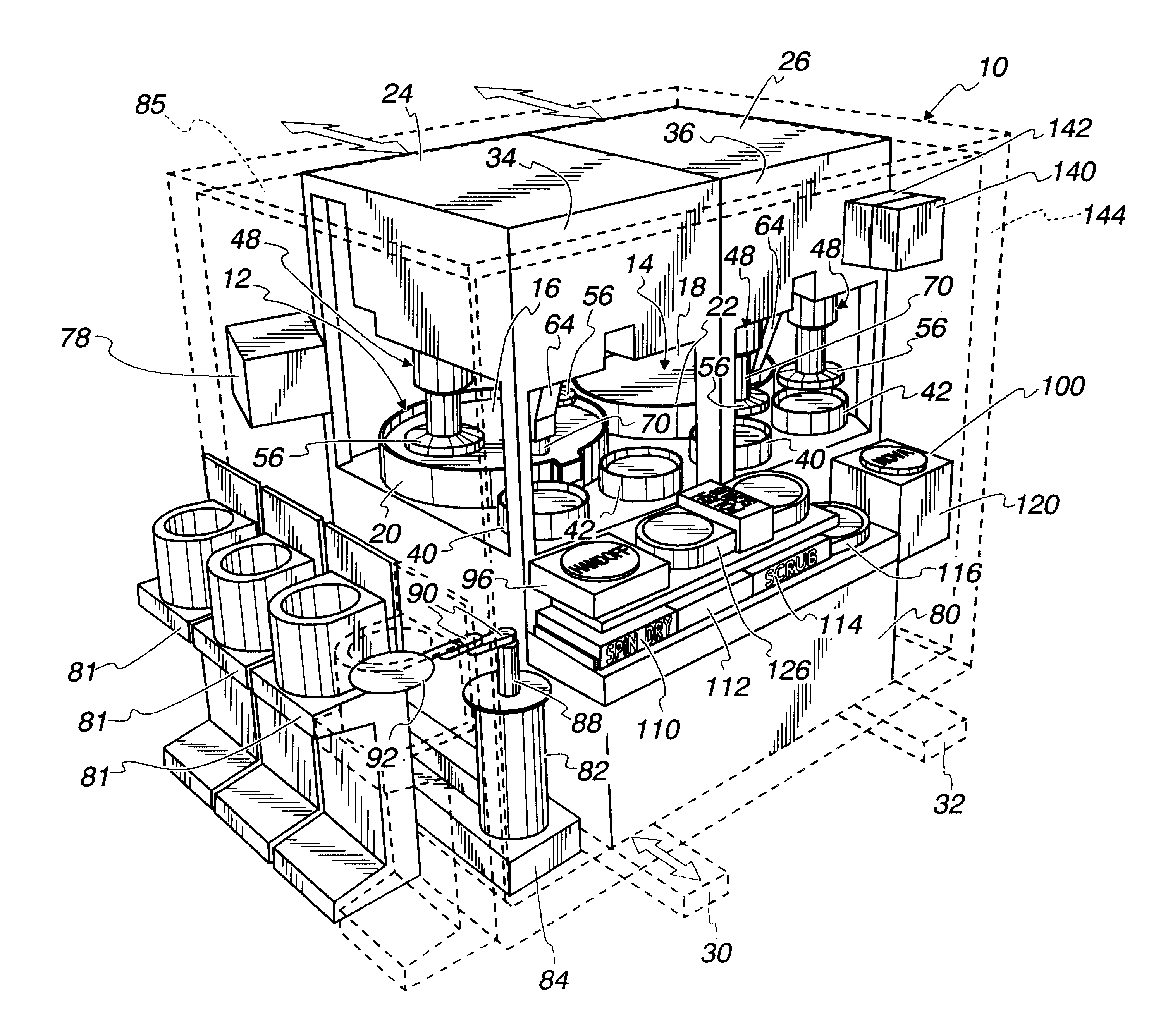
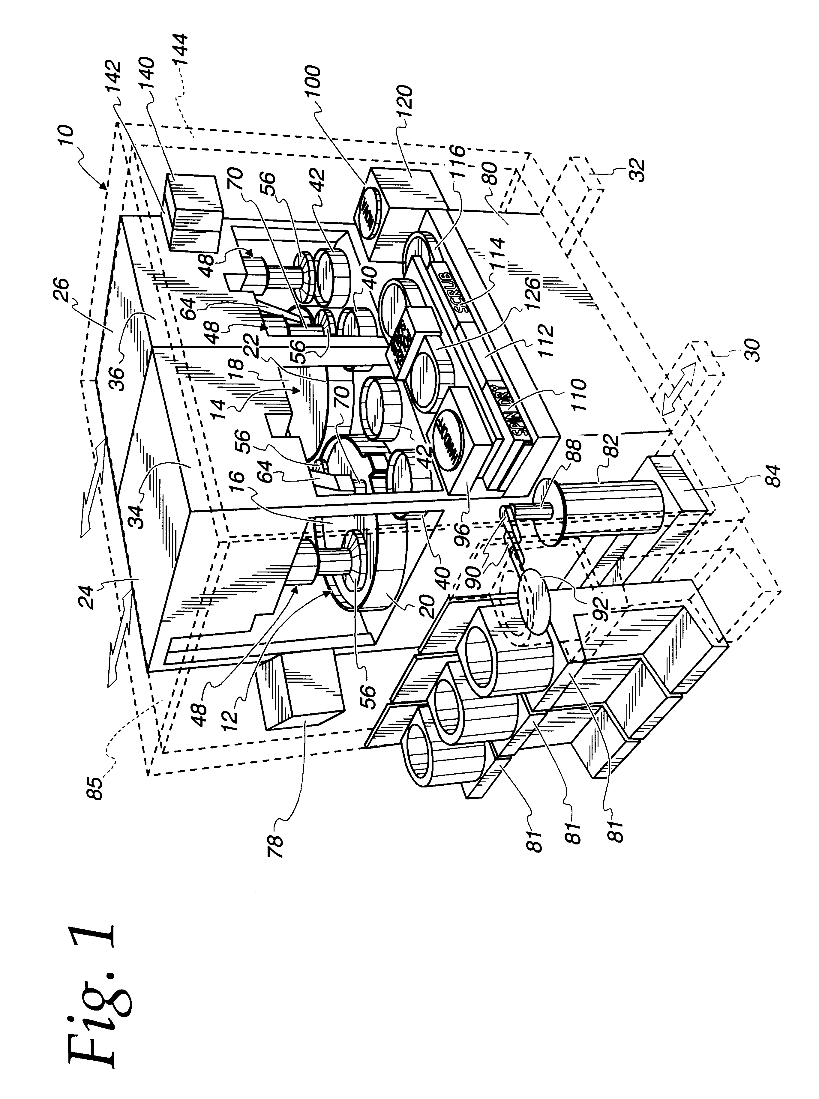
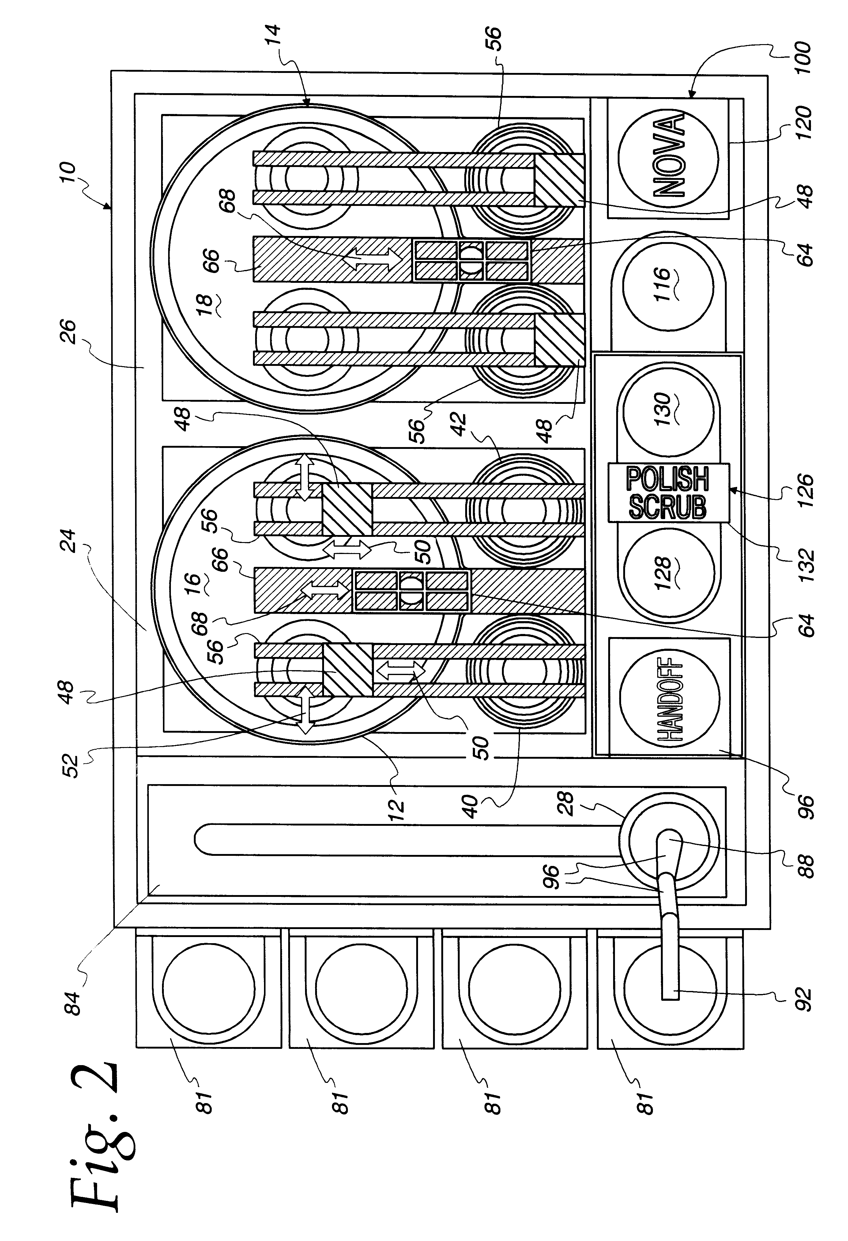
Referring now to the drawings, and initially to FIGS. 1 and 2, wafer processing apparatus according to principles of the present invention is generally indicated at 10. As will be seen herein, apparatus 10 is provided for performing a number of varied operations in a commercial wafer production environment. Apparatus 10 include two platen arrangements 12, 14 which include polishing surfaces 16, 18 and upstanding outer walls 20, 22 rising slightly above the working surfaces 16, 18 for slurry containment. The platen arrangements 12, 14 are located within respective polishing modules 24, 26. The modules 24, 26 are separate and independent from one another and are connected with a "backbone" or "docking" structure enclosed in a cabinet 80. Preferably, the "backbone" includes a framework (with valves and switches) supporting a plurality of flexible hoses for gas and liquid, and flexible cables for electrical power and electrical signals. The hoses and cables are connected to nearby modul...


PUM

PropertyMeasurementUnit
Pressureaaaaaaaaaa

Abstract

Wafer polishing systems include a series of polish modules alongside a neighboring series of secondary modules. A conveyor travels along the series of polish modules and the series of secondary modules. When a polishing operation is completed, the wafers are transferred to a series of near-by storage modules. The polish modules include a pair of traveling wafer gantries, each of which delivers a wafer to a polishing surface, applying the necessary force to complete polishing of the wafer surface.

Description

BACKGROUND OF THE INVENTION1. Field of the InventionThe present invention pertains to the polishing of wafers, especially wafers of semiconductor material bearing electronic circuit elements.2. Description of the Related ArtThe production of semiconductor devices, such as integrated circuits, begins with the preparation of high quality raw semiconductor wafers. Because of the relative purity of the semiconductor material, even the raw, unprocessed semiconductor wafers have a substantial cost. Thin layers of expensive materials are then stacked on top of a raw silicon wafer and then on top of one another in succession. A variety of carefully controlled operations such as metalization, sputtering, and ion implantation are used to form the respective layers. The thickness of the layers is relatively small, typically on the on the order of several molecular dimensions.During integrated circuit production, as circuit layers are successively stacked one on top of the other, an extremely f...

Claims


Application Information

Patent Timeline
IPC IPC(8): B24B41/00B24B37/04H01L21/00B24B37/34H01L21/687
CPCB24B37/345B24B41/005H01L21/67219H01L21/68707
Inventor BOWMAN, MIKE L.HEMPEL, GENEKARLSRUD, CHRISROOT, FRANKLIN D.
Owner NOVELLUS SYSTEMS
Why Eureka
Try Eureka