Method of equalizing device heights on a chip

a technology chips, applied in the field of equalizing device heights on chips, can solve the problems of limited success in growing epitaxial layers of iii-v materials that do support light emission, ineconomical feasibility of two such dissimilar devices, and problems such as the integration of optoelectronic devices with silicon

Inactive Publication Date: 2001-11-13
ALTERA CORP
View PDF4 Cites 20 Cited by
  • Summary
  • Abstract
  • Description
  • Claims
  • Application Information

AI Technical Summary

Problems solved by technology

Silicon CMOS is the most advanced today for many applications but the integration of optoelectronic devices with silicon has proved to be problematic for several reasons.
In addition, there has been limited success in growing epitaxial layers of III-V materials that do support light emission, such as gallium arsenide (GaAs) or indium phosphide (InP), on silicon substrates because of problems including the lattice mismatch.
It is not economically feasible for two such dissimilar...

Method used


Image

  • Method of equalizing device heights on a chip
  • Method of equalizing device heights on a chip
  • Method of equalizing device heights on a chip

Examples


Embodiment Construction

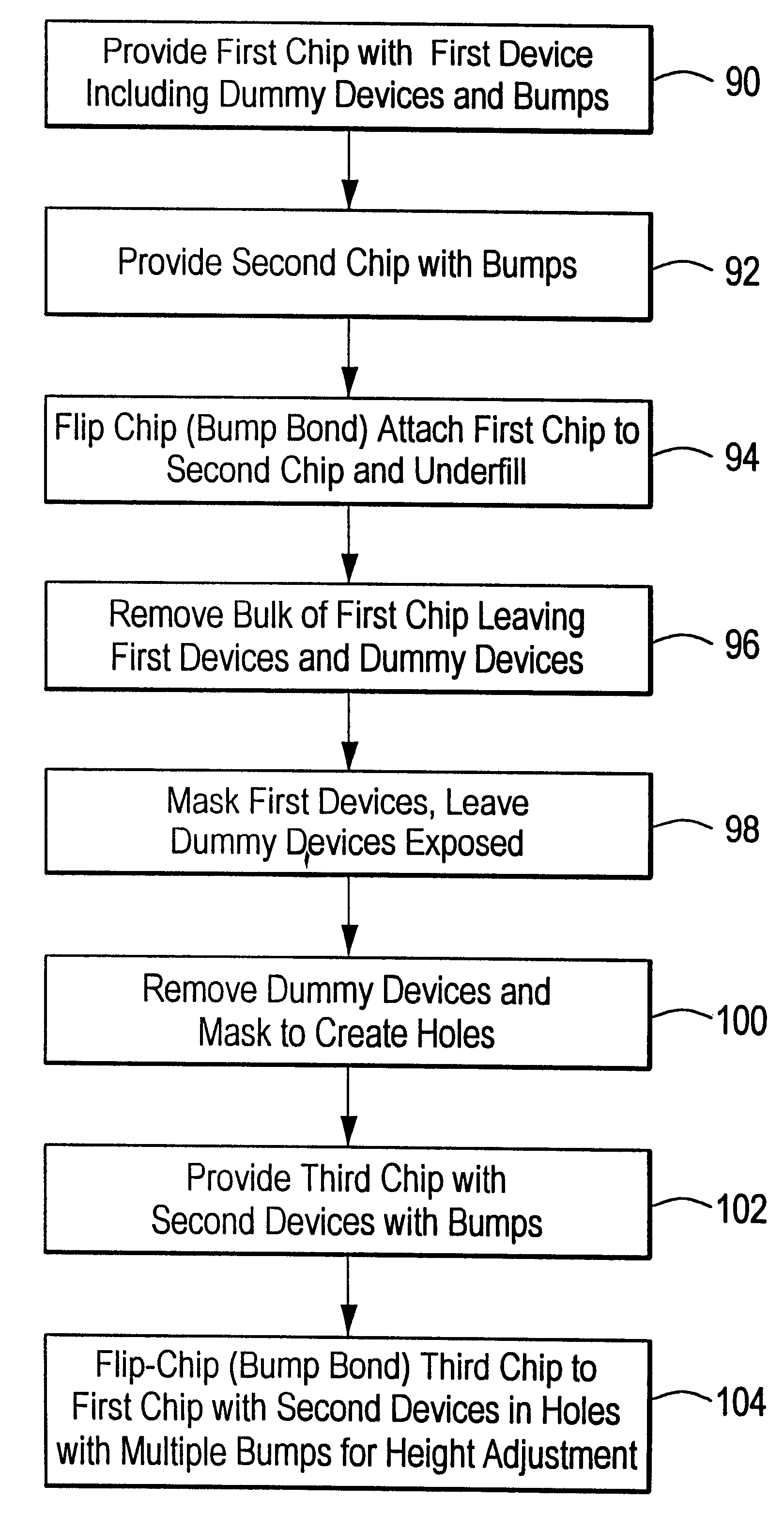
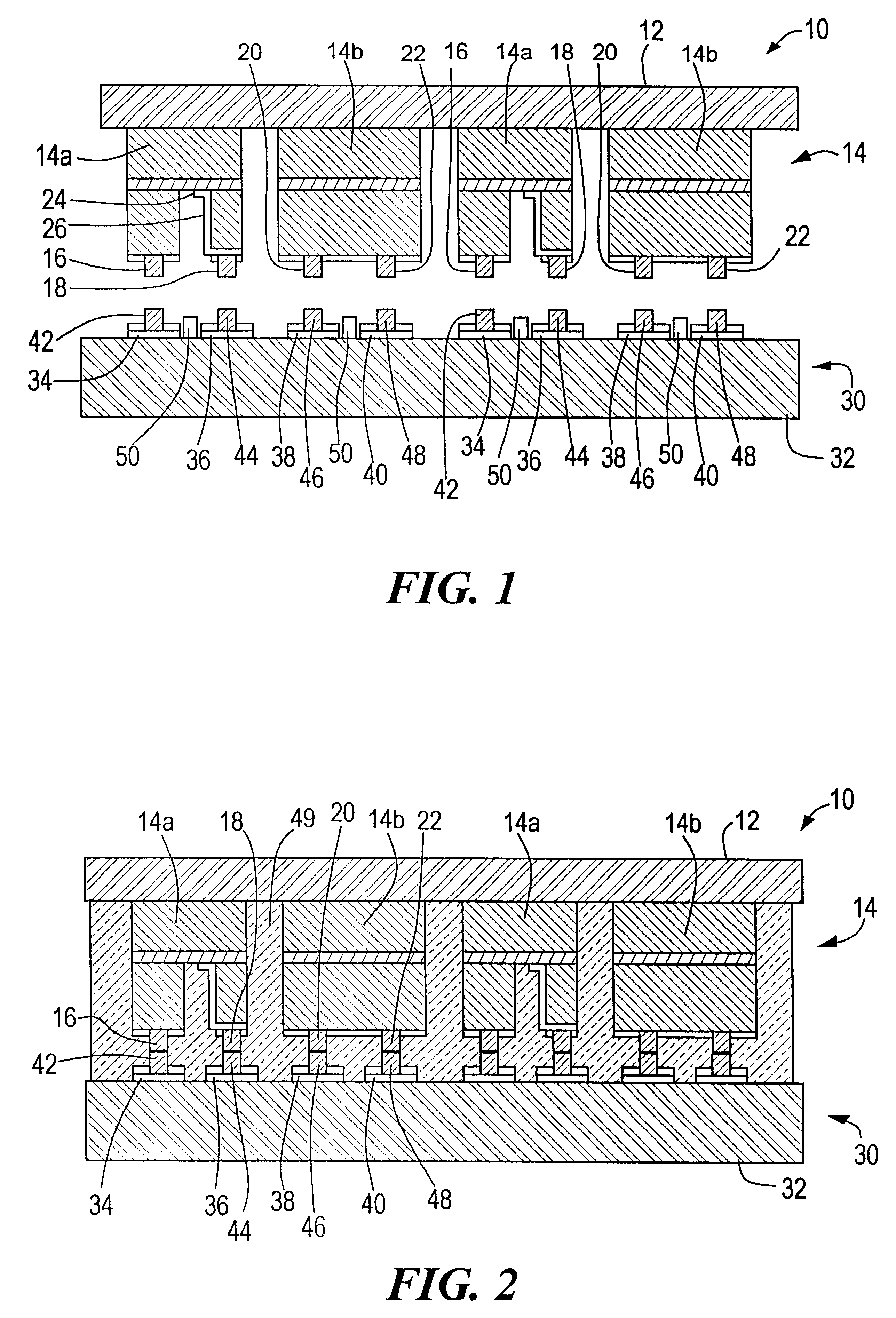
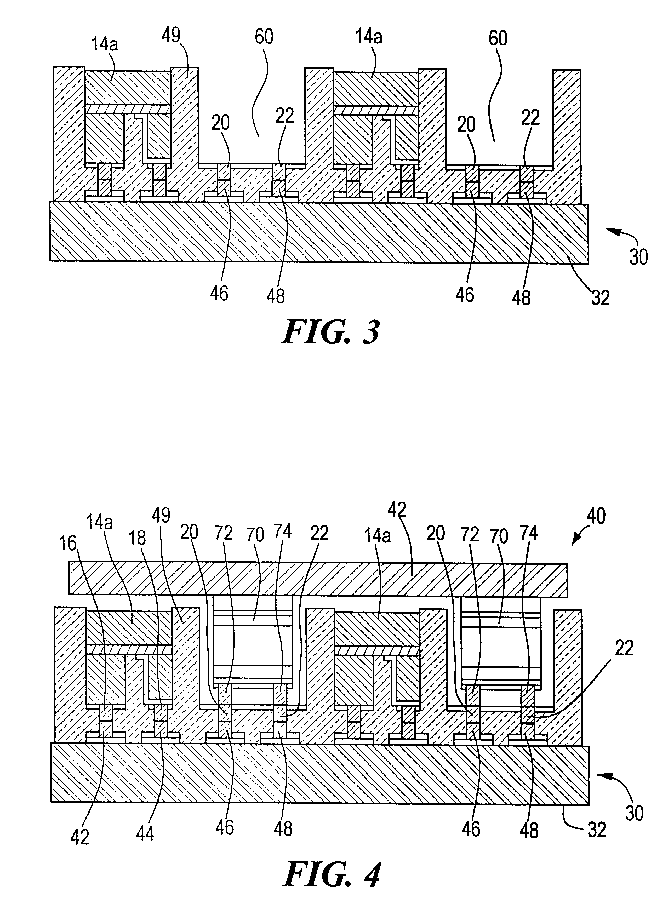
There is shown in FIG. 1 a first chip 10 including a gallium arsenide (GaAs) substrate on which has been grown a number of devices 14. These devices include a number of real, active devices 14a as well as dummy devices 14b. The real devices may be any type of device usable on an integrated circuit. The dummy devices may be simply more of the real devices which are to be sacrificed or other devices that are convenient to make or simply blanks or anything else which can reserve the space for future use. In this particular embodiment they are preferably photonic devices. More particularly they may be emitters or detectors and in this specific embodiment, the devices are vertical cavity surface emitting lasers (VCSELs). The VCSELs 14a and the dummies 14b which are also VSCELs are all grown together on the gallium arsenide substrate 12. The dummy devices 14b here are identical to the real devices 14a because they have all been grown together. This is for convenience only and the dummy de...


PUM


Abstract

A method of equalizing device heights on a chip includes providing on a first chip an array of first devices having a predetermined height including dummy devices with bonding bumps; engaging the bonding bumps on the first chip with those on the second chip; removing the dummy devices to create holes containing the double bumps previously associated with the dummy devices; providing on a third chip an array of second devices having a lower height than the first devices with bonding bumps which match those in the holes; and bump bonding the third chip to the second chip with the second devices in the holes and the bonding bumps on the second devices combining with the multiple bumps in the holes to equalize the height of the first and second devices.

Description

This invention relates to an improved method of equalizing device heights on a chip and more particularly for planarizing device heights in flip-chip bump bonded chips.BACKGROUND OF INVENTIONHybrid CMOS silicon (Si) and gallium arsenide (GaAs) chip technology, also known as flip-chip, has been developed that allows for direct optical input / output from fiber bundles onto logic circuits. The integration of flip-chip technology with electronics is not limited to Silicon CMOS. The integration process would be the same using other substrates, integrated circuits, etc., such as silicon-germanium, gallium arsenide or other semiconductors, including binary, ternary and quaternary compounds. Silicon CMOS is the most advanced today for many applications but the integration of optoelectronic devices with silicon has proved to be problematic for several reasons. Silicon does not have the band-gap structure that supports the generation of light. In addition, there has been limited success in gro...

Claims


Application Information

Patent Timeline
IPC IPC(8): G02B6/42G02B6/43H04B10/12
CPCG02B6/4249G02B6/4292G02B6/43G02B6/4246H01L2221/68359H01L2221/68363H01L2224/16225
Inventor TREZZA, JOHN A.
Owner ALTERA CORP
Why Eureka
Try Eureka