Method for eliminating transfer gate sacrificial oxide

a technology of transfer gate and sacrificial oxide, which is applied in the direction of semiconductor devices, basic electric elements, electrical equipment, etc., can solve the problems of high product cost, problems such as the above-described conventional method, and the difficulty of subsequent processing

Inactive Publication Date: 2002-01-29
INT BUSINESS MASCH CORP
View PDF11 Cites 5 Cited by
  • Summary
  • Abstract
  • Description
  • Claims
  • Application Information

AI Technical Summary

Benefits of technology

With the invention, an entire oxide strip step is eliminated, which reduces the removal of the isolation fill feature (especially thermal oxide etches). Excessive oxide removals can damage the substrate surface, degrade the gate integrity / reliability, and cause defects, thereby creating complications during subsequent processing.
The present invention also improves seams, polysilicon-to-polysilicon shorts yields, reduces the corner device leakage, and rounds the corners of the trench isolations, all of which have significant MOSFET performance implications.

Problems solved by technology

However, the above-described conventional method is problematic because the combination of these isotropic wet etches for removing the pad nitride, pad oxide, and TG Sac Ox consumes isolation oxides.
In STI isolation, the weak points in the TEOS fill create problems for subsequent processing when exposed during prior processing.
Thus, additional stripping steps result in high product costs due to defective parts.
Field oxide isolation processing also has certain defects associated therewith including oxide consumption, leakage, poor insulation and a "corner device".
The thermal oxide isotropic etches are particularly harmful for causing the isolation pull-down, the "seam", and "divot".
As a result, the divots are formed at corners of the trench fill which creates later processing problems by making the surface of the wafer less planar.
The non-planar wafer surface causes photolithography problems, film uniformity issues, and increases the risk of process defects such as PC-PC shorts, or entrapment of foreign material.
Excessive oxide removals can damage the substrate surface, degrade the gate integrity / reliability, and cause defects, thereby creating complications during subsequent processing.

Method used


Image

  • Method for eliminating transfer gate sacrificial oxide
  • Method for eliminating transfer gate sacrificial oxide
  • Method for eliminating transfer gate sacrificial oxide

Examples


Embodiment Construction

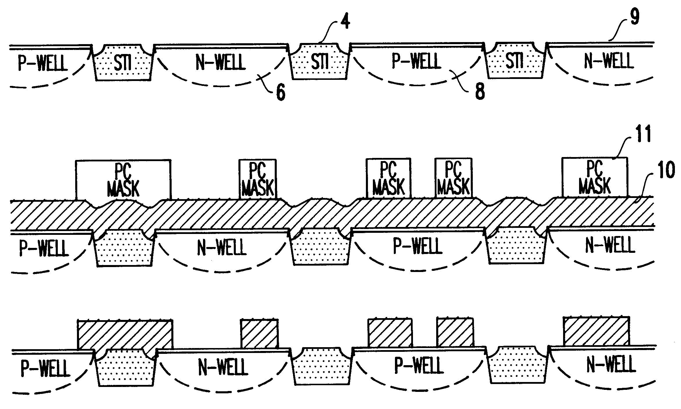
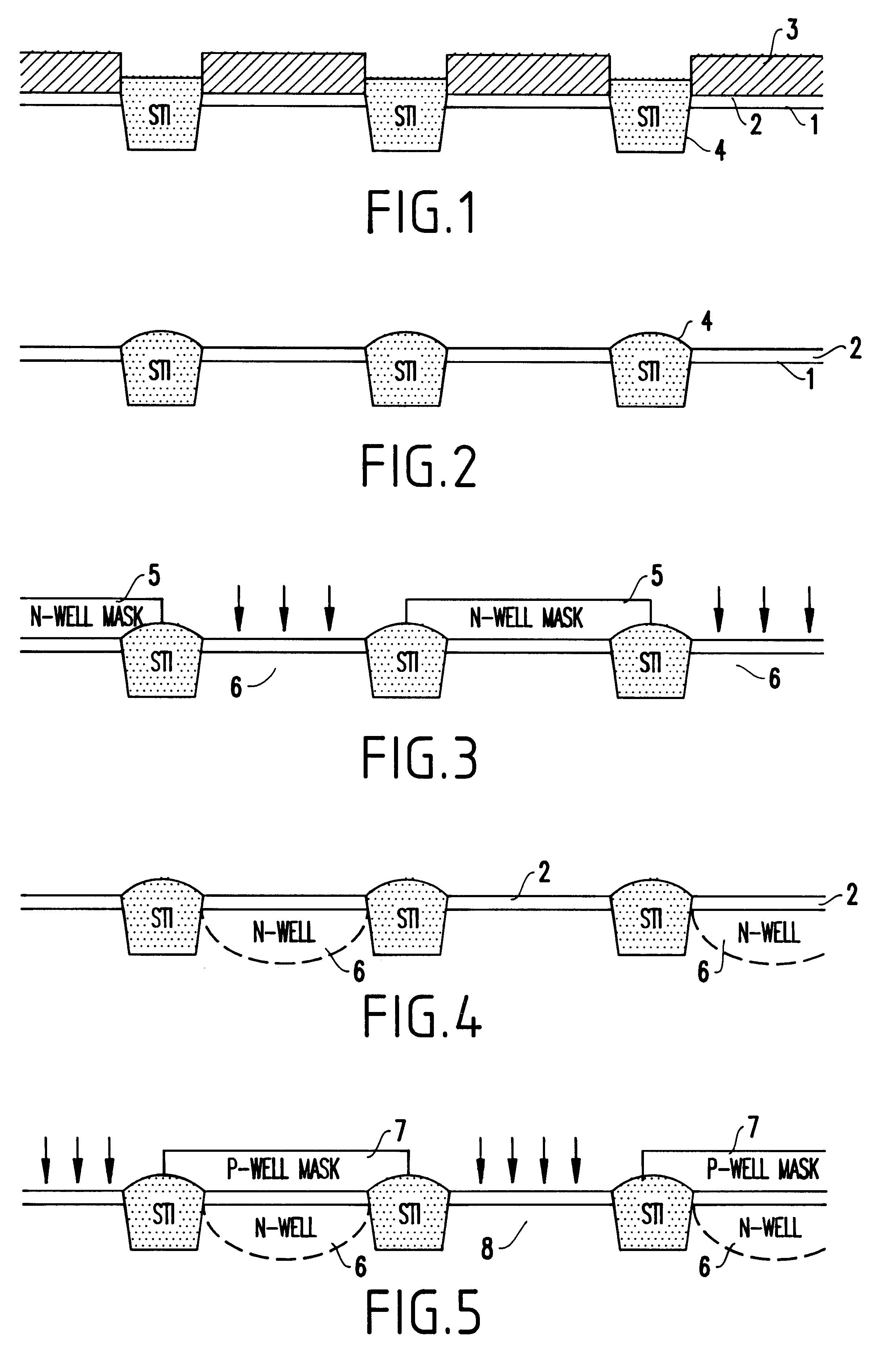
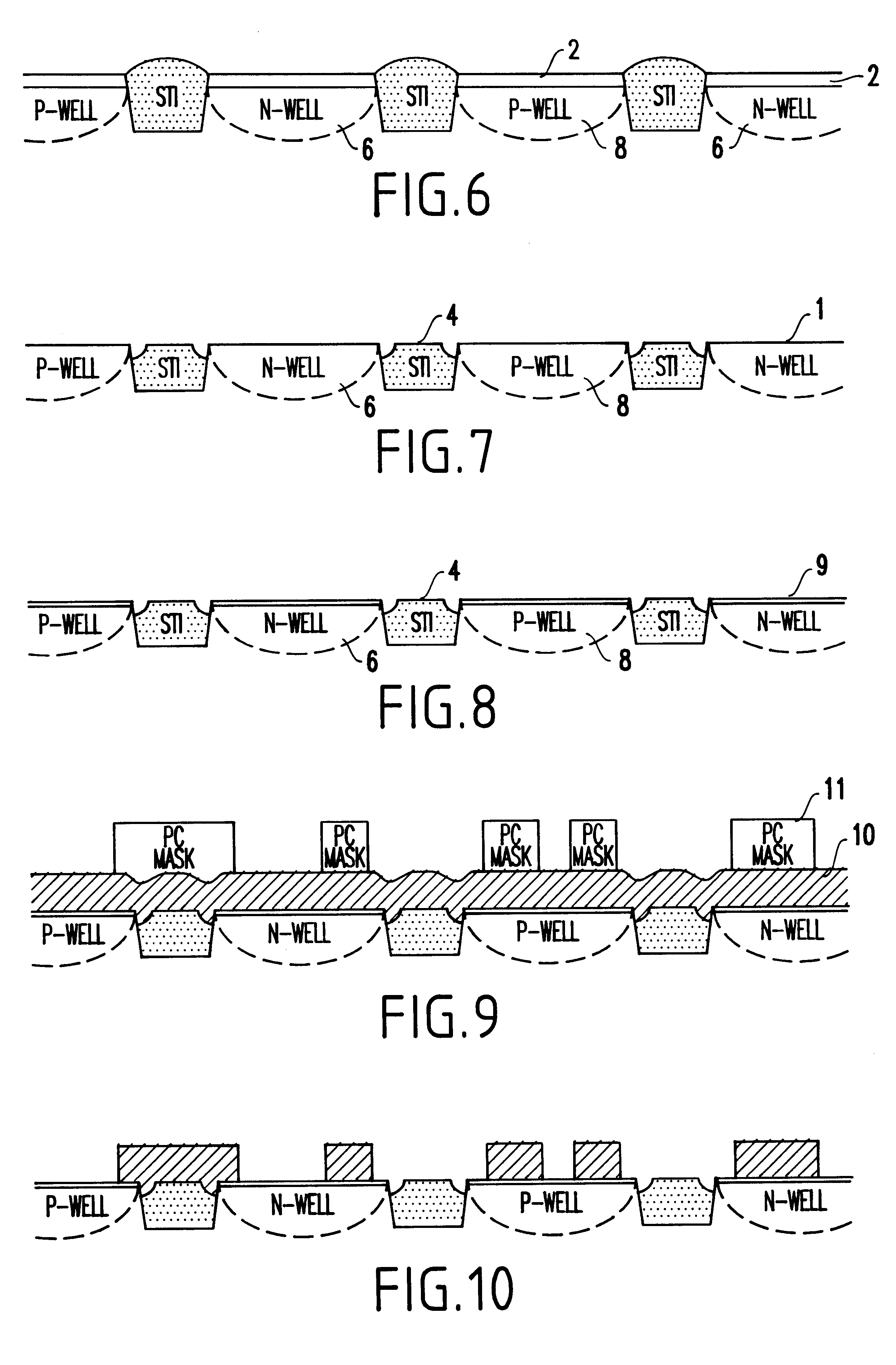
The first preferred embodiment of the present invention eliminates the transfer gate sacrificial oxide and the associated steps from the conventional process as described above. Specifically, this process uses the initial pad oxide (e.g., the oxide in an isolation pad stack) as a screen film for the well implants. For instance, if this pad oxide is beneath nitride in a stack, using a selective, well-controlled wet (e.g., hot phosphoric acid etch) or dry etch (e.g., CDE), the nitride is removed, and the pad oxide is etched to the desired thickness to perform the well ion implants. Thus, the invention eliminates an entire oxide removal step, traditionally used to expose the Si substrate before forming desired thickness screens. This invented process will reduce significantly the corner divot, trench center pulldown, and synergistically reduce the chance of exposing STI trench voids which lead to polysilicon shorts in the isolation, as shown in a comparison of FIGS. 11 and 12, with FIG...


PUM

PropertyMeasurementUnit
thicknessaaaaaaaaaa
thicknessaaaaaaaaaa
thicknessaaaaaaaaaa

Abstract

A method of forming a semiconductor device, includes forming a layer of oxide on a semiconductor substrate, forming a layer of silicon nitride on the oxide layer, forming isolation regions in the substrate using the oxide layer and the nitride layer, removing the silicon nitride layer, ion implanting dopant ions using the original oxide layer as a screen, into the substrate, and removing the oxide layer and forming a gate oxide layer over the substrate. Another method of forming an active area of a semiconductor device, includes using a pad oxide, remaining after removing a film layer thereover of an oxide / film mask stack, for a screen layer for well implants formed in the substrate, removing the oxide layer and forming a gate oxide over the substrate, following defining the well implants, without using a sacrificial oxide.

Description

1. Field of the InventionThe present invention relates to a method of forming a semiconductor device, and more particularly to a method of fabrication, which eliminates the need for transfer gate sacrificial oxide, thereby reducing the number of process steps in forming metal oxide semiconductor field effect transistors (MOSFETs), improving corner device leakages, reducing process defects, and loss of isolation insulator material.2. Description of the Related ArtIn processing a logic wafer, the initial step is forming an oxide (e.g., typically referred to as a "pad oxide"), and thereafter depositing a silicon nitride layer (e.g., typically referred to as a "pad nitride"), creating an isolation feature (e.g., a shallow trench isolation, but equally relevant to a field oxide isolation or other means of isolation), and filling the trench with insulator material.Next, the pad nitride is stripped, typically using a hot phosphoric etch, followed by a hydrofluoric acid (HF) dip, or any oxi...

Claims


Application Information

Patent Timeline
Patent Type & Authority Patents(United States)
IPC IPC(8): H01L21/02H01L21/762H01L21/70H01L21/28H01L21/8238H01L21/316H01L21/314H01L21/335
CPCH01L21/28167H01L21/76224H01L21/823878H01L21/823892H01L21/022H01L21/02164H01L21/18H01L21/31612H01L21/3143
Inventor HOULIHAN, KEVIN M.RANKIN, JED H.
Owner INT BUSINESS MASCH CORP
Why Eureka
Try Eureka