Molding a polishing pad having integral window

a polishing pad and window technology, applied in the field of polishing pads, can solve the problems of determining when the wafer has been polished, higher scrap rate and production costs, and leakage of slurry between the polishing pad and the window piece,

Inactive Publication Date: 2002-05-14
ROHM & HAAS ELECTRONICS MATERIALS CMP HLDG INC
View PDF9 Cites 78 Cited by
  • Summary
  • Abstract
  • Description
  • Claims
  • Application Information

AI Technical Summary

Problems solved by technology

One problem associated with chemical-mechanical polishing is determining when the wafer has been polished to the desired degree of flatness.
Further, if a critical wafer dimension is found to be below a prescribed minimum, the wafer may be unusable, thereby leading to higher scrap rates and production costs.
Leakage of slurry between the pad and the window piece may be a problem.
Also, since the window material is different than the pad material, the window and the pad may wear at different rates.
This may lead to cracking or tearing of the pad around the window during polishing.

Method used


Image

  • Molding a polishing pad having integral window
  • Molding a polishing pad having integral window

Examples


Embodiment Construction

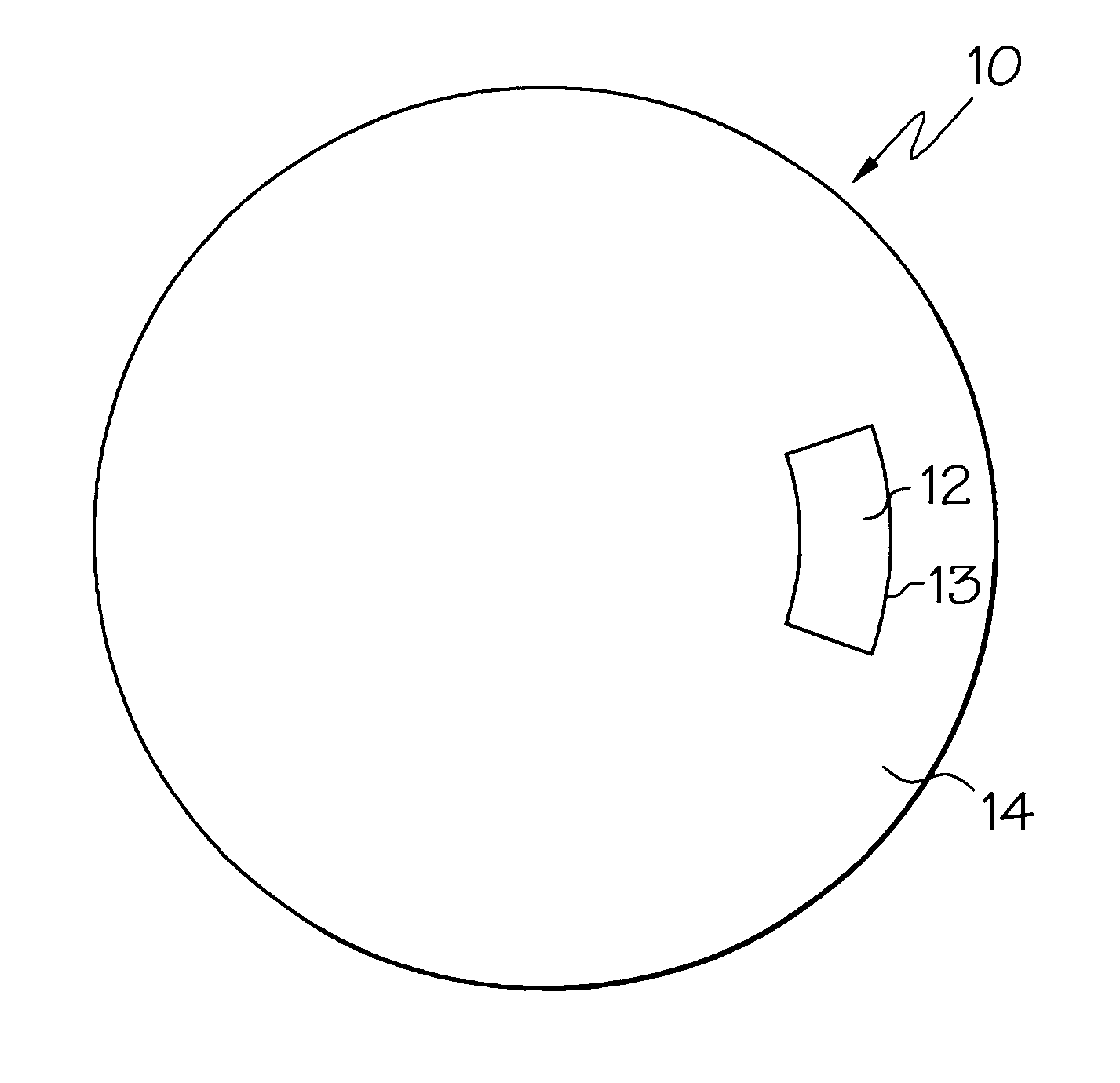
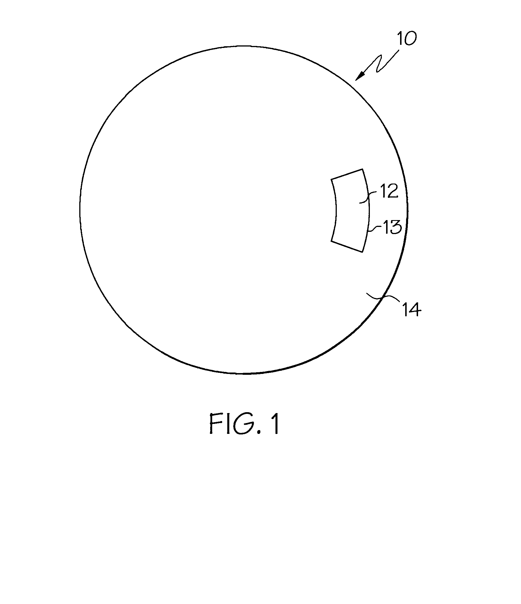
A polishing pad according to the invention as shown in FIG. 1 comprises a one-piece molded article 10 which is shaped as a substantially flat disk having opposite major surfaces. One of the major surfaces is a polishing surface that is applied to a workpiece during polishing, and the other major surface is a back surface that is contacted by a platen on which the polishing pad is mounted, either directly or through an intermediate base pad.

The molded polishing pad is characterized by a region 12 wherein the polymeric material is transparent. By transparent it is meant that the region exhibits transmissivity on the order of 20% or more to an incident light beam having some wavelength in the range from infrared to ultra-violet, at least when the light beam is at an angle of incidence substantially normal to the surface of the polishing pad. It should be understood that the transparent region need not be totally transmissive, and that some scattering of incident light, particularly due...


PUM

PropertyMeasurementUnit
thicknessaaaaaaaaaa
mold temperatureaaaaaaaaaa

Abstract

A polishing pad is formed by solidifying a flowable polymeric material at different rates of cooling to provide a polishing pad with a transparent region and an adjacent opaque region. Types of polymeric material suitable for making the polishing pad include a single thermoplastic material, a blend of thermoplastic materials, and a reactive thermosetting polymer.

Description

1. Field of the InventionThis invention relates to a polishing pad which is useful for creating a smooth, ultra-flat surface on such items as glass, semiconductors, dielectric / metal composites, and integrated circuits. More particularly, the invention relates to a molded polishing pad having a window which facilitates inspection of a workpiece and determination of a polishing endpoint by optical means.2. Discussion of Related ArtSemiconductor wafers having integrated circuits fabricated thereon must be polished to provide a very smooth and flat wafer surface which in some cases may vary from a given plane by as little as a fraction of a micron. Such polishing is usually accomplished in a chemical-mechanical polishing (CMP) operation which utilizes a chemically active slurry that is buffer against the wafer surface by a polishing pad.One problem associated with chemical-mechanical polishing is determining when the wafer has been polished to the desired degree of flatness. Conventiona...

Claims


Application Information

Patent Timeline
Patent Type & Authority Patents(United States)
IPC IPC(8): B24D3/20B24D7/00B24D3/28B24D7/12B24B37/04B24D13/00B24D13/14B24B37/20
CPCB24D3/28B24B37/205B24D11/00
Inventor ROBERTS, JOHN V. H.PINHEIRO, BARRY SCOTTJAMES, DAVID B.
Owner ROHM & HAAS ELECTRONICS MATERIALS CMP HLDG INC
Why Eureka
Try Eureka