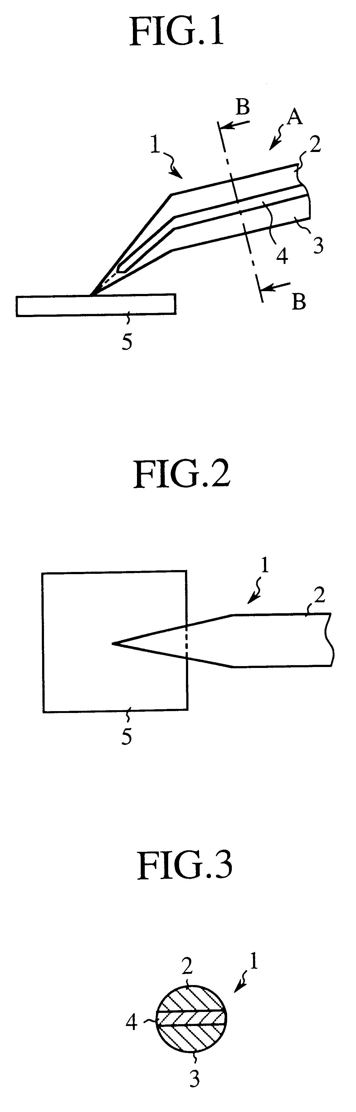
Probe stylus

a technology of probe stylus and probe card, which is applied in the direction of measurement devices, semiconductor/solid-state device testing/measurement, instruments, etc., can solve the problem of difficult setting of the prior art probe stylus onto the probe card

Inactive Publication Date: 2002-06-11
MITSUBISHI ELECTRIC CORP
View PDF11 Cites 96 Cited by
  • Summary
  • Abstract
  • Description
  • Claims
  • Application Information

AI Technical Summary

Problems solved by technology

However, the setting of the probe styluses of the prior art onto a probe card is difficult when a large number of pads are disposed in a semiconductor device.

Method used


Image

  • Probe stylus
  • Probe stylus
  • Probe stylus

Examples


fourth embodiment

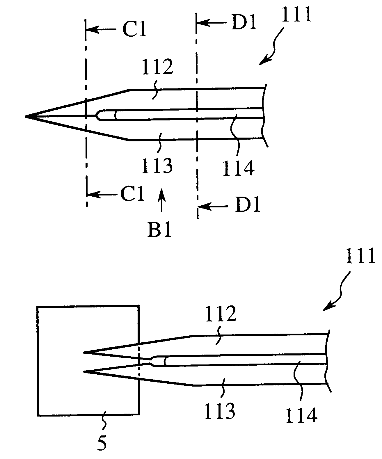
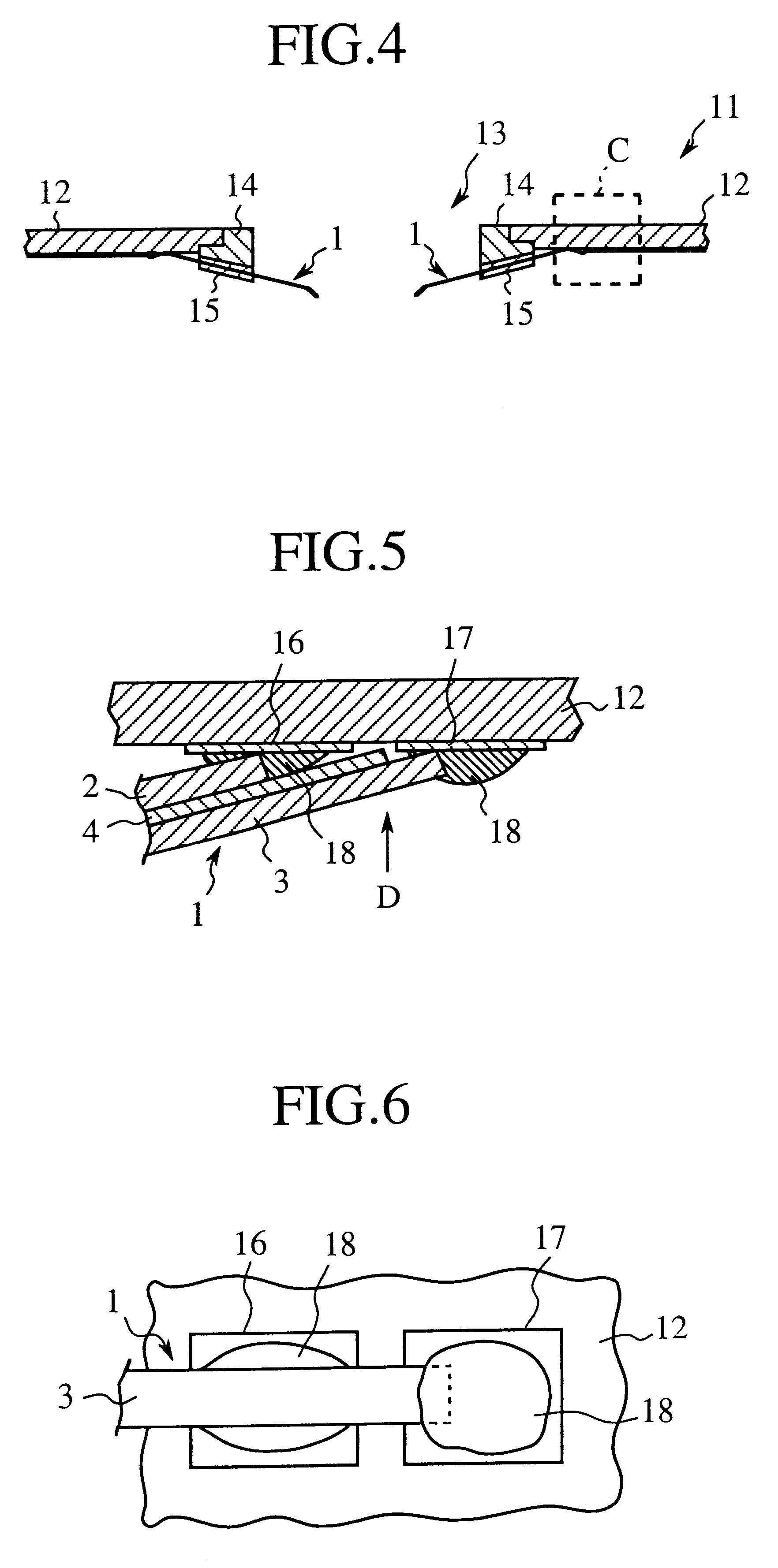
In a probe stylus according to the third embodiment, the first and second electrically conductive members 2b, 3b are connected at their tip. On the other hand, in a probe stylus according to the fourth embodiment of the present invention, the first and second electrically conductive members are not connected at their tip. And at an inspection of a semiconductor device, they are connected to each other through a pad disposed in the semiconductor device. The other feature is similar to that of the third embodiment.

FIG. 13 shows that the probe stylus 1c is contacting with a pad 5 disposed in a semiconductor device. Referring to the figures, reference numerals 1c, 2c, 3c denote a probe stylus, a first electrically conductive member, and a second electrically conductive member, respectively. The first and second electrically conductive members 2c, 3c are connected by an insulating member 4c arranged between them. Reference numeral 5 denotes a pad disposed in a semiconductor.

The structure...

fifth embodiment

FIG. 15 shows that the probe stylus 21 is contacting with a pad 5 disposed in a semiconductor device. Referring to the figure, reference numerals 21, 22, 23 denote a probe stylus, a first electrically conductive member, and a second electrically conductive member, respectively. The first and second electrically conductive members 22, 23 are connected by an insulating member 24 arranged between them. Reference numeral 5 denotes a pad disposed in a semiconductor device.

The probe stylus 21 of the fifth embodiment of the present invention is a so-called perpendicular type probe stylus. Each of the first and second electrically conductive members 22, 23 has a form of needle. The cross section perpendicular to the longitudinal direction of the needle is half round. Namely, each of the first and second electrically conductive member 22, 23 has a form of a conventional perpendicular type probe stylus divided equally along its longitudinal axis. Thus, the assembly of the probe stylus of the ...

sixth embodiment

In a probe stylus according to the fifth embodiment, the first and second electrically conductive members 22, 23 are connected at their tip. On the other hand, in a probe stylus according to the sixth embodiment of the present invention, the first and second electrically conductive members 22, 23 are not connected at their tip. And at an inspection of a semiconductor device, they are connected to each other through a pad disposed in a semiconductor device. The other feature is similar to that of the fifth embodiment.

FIG. 20 shows that the probe stylus 21a is contacting with a pad 5 disposed in a semiconductor device. Referring to the figure, reference numerals 21a, 22a, 23a denote a probe stylus, a first electrically conductive member, and a second electrically conductive member, respectively. The first and second electrically conductive members 22a, 23a are connected by an insulating member 24a arranged between them. Reference numeral 5 denotes a pad disposed in a semiconductor.

The...


PUM


Abstract

The present invention relates to a probe stylus 1 for an inspection of semiconductor device in a state of wafer. When a large number of pad 5 are disposed in a semiconductor device, setting of the probe styluses 1 onto a probe card, on which a semiconductor to be inspected shall be mounted, is difficult. An objet of the present invention is to improve the form of the probe stylus to solve this problem.The object is attained by a probe stylus according to the present invention. The probe stylus 1 is comprised of a first electrically conductive member 2, a second electrically conductive member 3, and an insulating member 4 disposed between the first and second electrically conductive members 2,3, wherein the first and second electrically conductive members 2,3 have a form of a needle and they form a single needle. In an embodiment, the first and second electrically conductive members have a half round cross section. In another embodiment, each of the first and second electrically conductive members has a resilient portion at their tip portion. In another embodiment, the first electrically conductive member is covered with the insulating member, and the insulating member is covered with the second electrically conductive member. In further another embodiment, a slit is disposed between the first and second electrically conductive members.

Description

1. Field of the InventionThe present invention relates to a probe stylus for inspecting a semiconductor at a wafer state.2. Description of the Prior ArtA probe stylus in the prior art is constituted by a single electrically conductive needle. In a high precision inspection of a semiconductor device at a wafer state, a probe styluses for applying force and probe styluses for sensing are connected to pads disposed in a semiconductor. These probe styluses are connected to form a Kelvin connection. In such probe styluses, a cantilever type probe stylus and a perpendicular type probe stylus are known. The cantilever type probe stylus contacts obliquely With a pad disposed in a semiconductor device, and the perpendicular type probe stylus contacts perpendicularly with a pad, at an inspection of a semiconductor.During an inspection of an I / O of a semiconductor device, for example, a high speed logic element, when an output data of a driver of a tester is inputted into a signal input termin...

Claims


Application Information

Patent Timeline
Patent Type & Authority Patents(United States)
IPC IPC(8): G01R1/067H01L21/66
CPCG01R1/0675G01R1/06738G01R1/06716G01R1/06761
Inventor NODA, HIROSHI
Owner MITSUBISHI ELECTRIC CORP
Why Eureka
Try Eureka