Method of manufacturing electron-emitting device, electron source and image-forming apparatus, and apparatus of manufacturing electron source

a technology of image-forming apparatus and electron-emitting device, which is applied in the manufacture of electrode systems, electric discharge tubes/lamps, and tube/lamp factory adjustment, etc., and can solve the problems of large-scale image-forming apparatus, insufficient activation, and too much time for activation process

Inactive Publication Date: 2002-07-16
CANON KK
View PDF14 Cites 12 Cited by
  • Summary
  • Abstract
  • Description
  • Claims
  • Application Information

AI Technical Summary

Problems solved by technology

Therefore, it takes too much time to perform the activation process.
Accordingly, there is a case in which lack of the organic substance during the activation process causes no sufficient activation.
A large-sized image-forming apparatus will bring serious problems.
However,

Method used


Image

  • Method of manufacturing electron-emitting device, electron source and image-forming apparatus, and apparatus of manufacturing electron source
  • Method of manufacturing electron-emitting device, electron source and image-forming apparatus, and apparatus of manufacturing electron source
  • Method of manufacturing electron-emitting device, electron source and image-forming apparatus, and apparatus of manufacturing electron source

Examples


embodiment 1

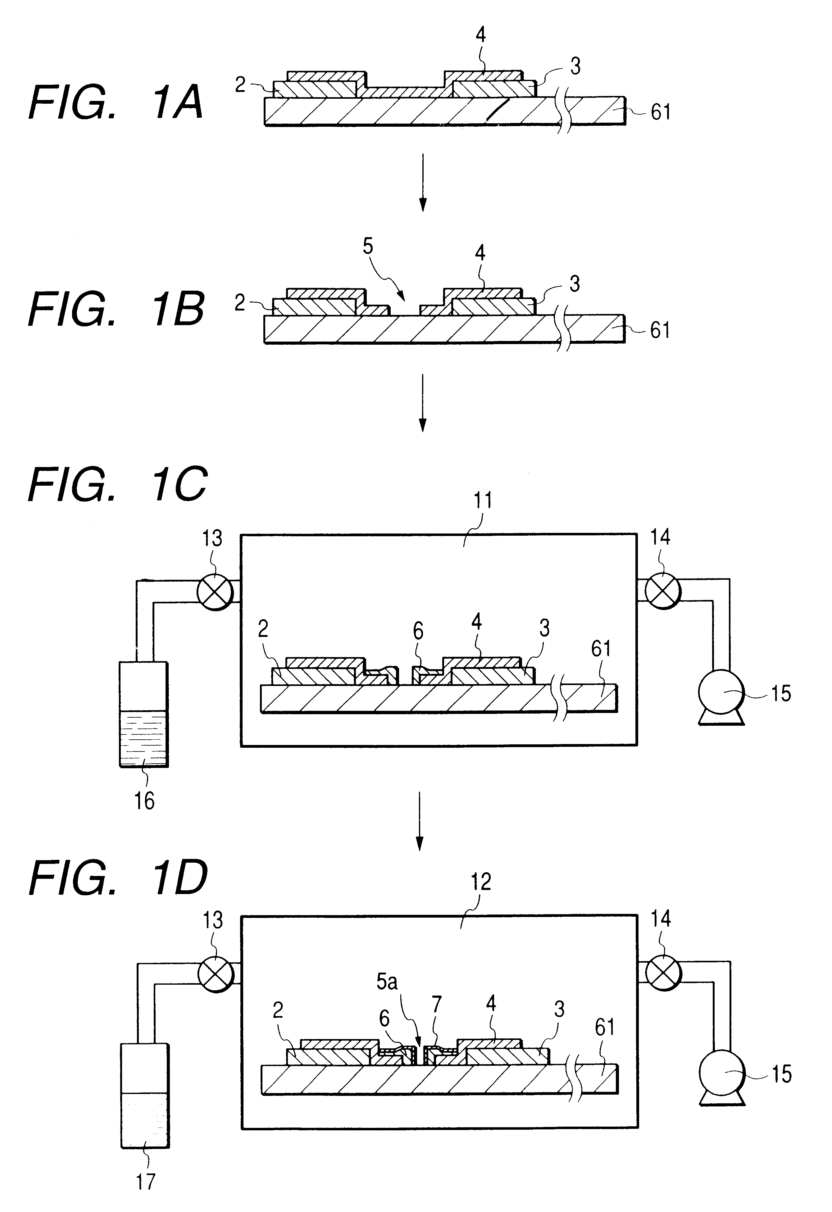
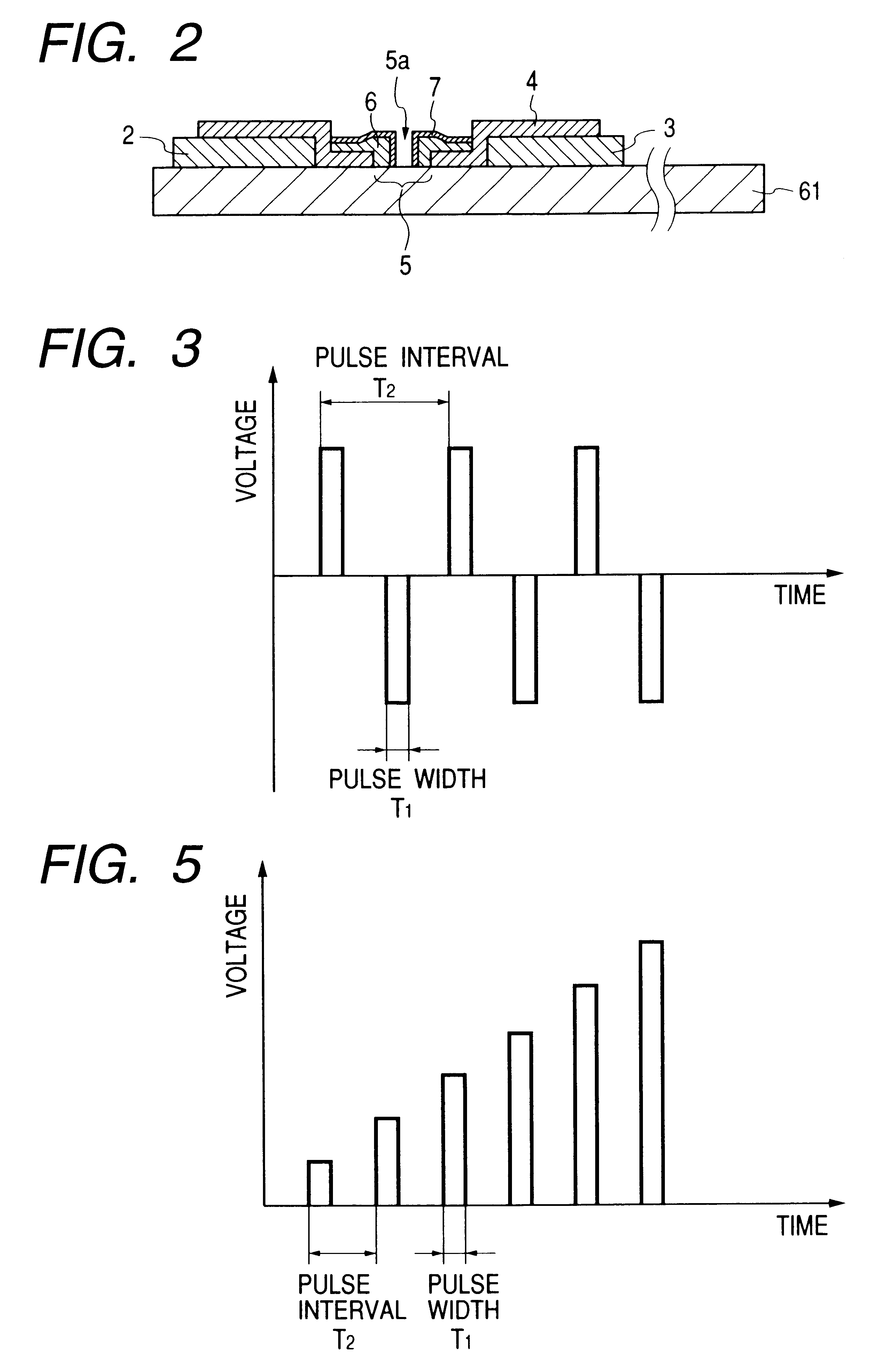
An electron source substrate is prepared, similar to Embodiment 1, and forming is performed.

The substrate is then set in the vacuum container 1202 of the activation device of FIG. 10, similar to Embodiment 1. After evacuating the inside of the vacuum container 1202, the valve 1226 and the valve 1227 are opened, and tornitrile is introduced into the vacuum container from the activation substance holding chamber 1219. The valve 1227 opening is regulated so that the partial pressure of tornitrile inside the vacuum container becomes 1.times.10.sup.-2 Pa. A voltage is then applied, similar to Embodiment 1, and the first activation is performed.

The valve 1226 and the valve 1227 are then closed, and after evacuating the inside of the vacuum container 1202 until the pressure becomes 5.times.10.sup.-6 Pa or less, the valve 1226 and the valve 1227 are once again opened, and tornitrile is introduced into the vacuum container from the activation substance holding chamber 1219. The valve 1227 op...

embodiment 2

has no noticeable dispersion in luminescence or uneven colors, and can display a good image which sufficiently satisfies its use as a television.

embodiment 3

Embodiment 3 is an example of another method of manufacture of an electron source.

An electron source substrate is formed in accordance with steps (a) to (d) of Embodiment 1. Flexible cables are mounted on the output lines of the X-direction wiring and the Y-direction wiring of the formed electron source substrate. Forming is then performed, similar to step (e) of Embodiment 1, forming an electron-emitting region.

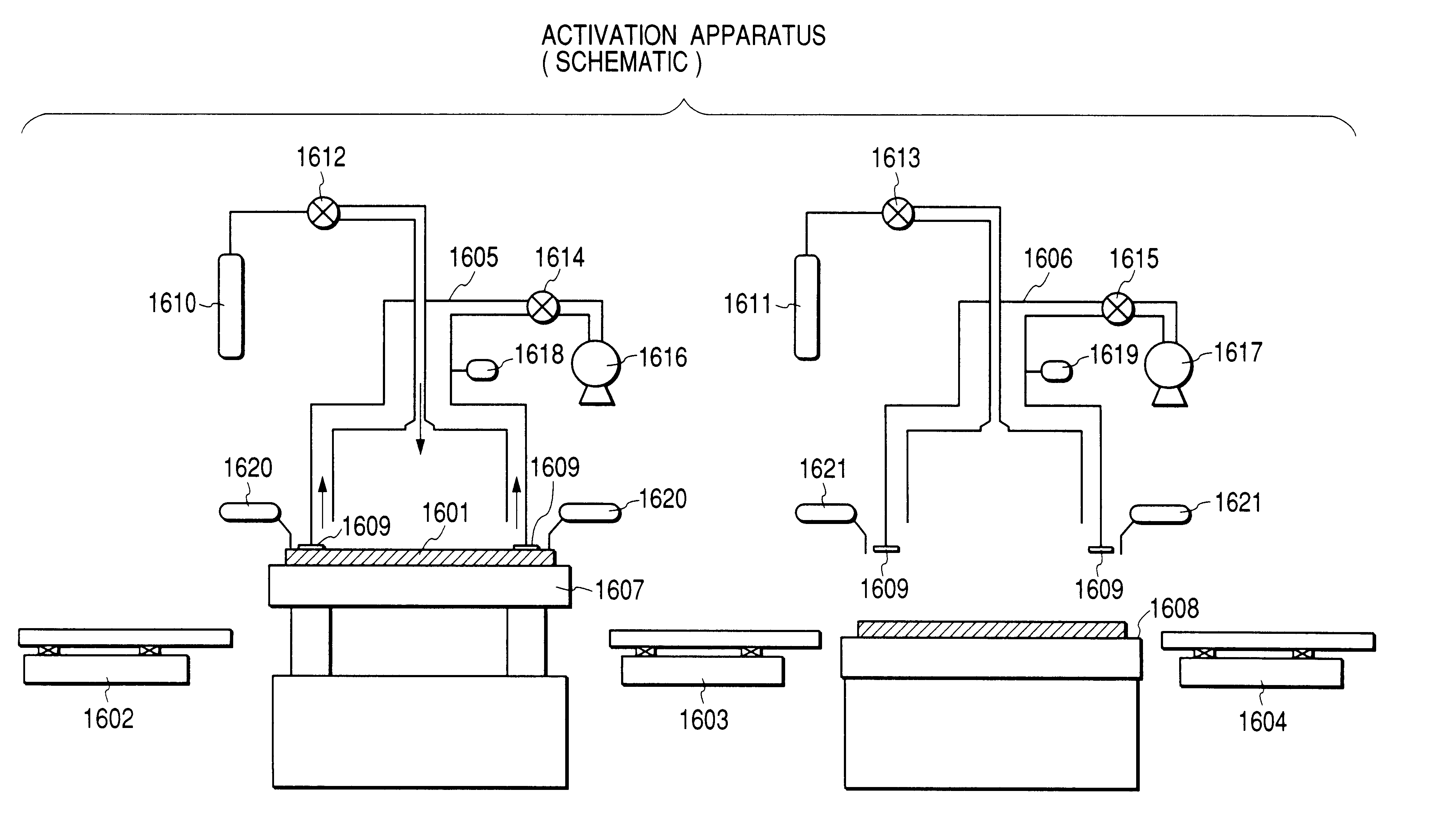
Next, activation of the electron source substrate 61 on which forming has been completed is performed using the activation device shown in FIG. 14.

The electron source substrate 61 is first set on a conveyor arm 1602 used for entry, and the electron source substrate 61 is then placed and fixed on a support member 1607 by using the conveyor arm 1602.

The support member 1607 is then raised, and the electron source substrate 61 and a first vacuum container 1605 are brought into contact. An airtight seal is maintained by an o-ring between the first vacuum container 1605 and the su...


PUM


Abstract

A method of manufacturing an electron-emitting device includes a process for forming a pair of electric conductors spaced from each other on a substrate, and an activation process for forming a film of carbon or a carbon compound on at least one of the pair of electric conductors. The activation process is sequentially performed within plural containers having different atmospheres.

Description

1. Field of the InventionThe present invention relates to a method of manufacturing an electron-emitting device, an electron source and an image-forming apparatus, and an apparatus of manufacturing the electron source.2. Related Background ArtTwo kinds of electron-emitting devices: a thermoelectron source and a cold cathode electron source are conventionally known. The types of the cold cathode electron-source include a field emission type (hereinafter abbreviated as an FE type) electron-emitting device, a metal / insulating layer / metal type (hereinafter abbreviated as a MIM type) electron-emitting device, and a surface conduction electron-emitting device.Known examples of the FE type are described by W. P. Dyke & W. W. Dolan in "Field emission" Advance in Electron Physics, 8, 89 (1956), by C. A. Spindt in "Physical Properties of thin-film field emission cathodes with molybdenum cones," J. Appl. Phys., 47, 5248 (1976), etc.In contrast to this, known examples of the MIM type are descri...

Claims


Application Information

Patent Timeline
IPC IPC(8): H01J9/02
CPCH01J9/027H01J9/12
Inventor TAMURA, MIKIOHNISHI, TOSHIKAZUJINDAI, KAZUHIRO
Owner CANON KK
Why Eureka
Try Eureka