Process of making carrier substrate and semiconductor device

a semiconductor and carrier substrate technology, applied in the field of semiconductor devices, can solve the problems of high production cost, complicated production process, and large area extending between inner and outer leads or mounting areas

Inactive Publication Date: 2002-07-23
SHINKO ELECTRIC IND CO LTD
View PDF4 Cites 62 Cited by
  • Summary
  • Abstract
  • Description
  • Claims
  • Application Information

AI Technical Summary

Problems solved by technology

A conventional semiconductor device, wherein a semiconductor chip mounted onto a lead frame is resin-shielded, has a problem in that an area extending between inner and outer leads or a mounting area is relatively large.
Further, in a BGA (ball grid array) type semiconductor device, there is another problem in that the production cost is high because it necessitates a substrate for mounting a semiconductor chip.
The repetition of the steps of coating the etching resist 61 onto the metallic substrate 60 and half-etching the same after being exposed and developed complicates the production process to increase the production cost.

Method used


Image

  • Process of making carrier substrate and semiconductor device
  • Process of making carrier substrate and semiconductor device
  • Process of making carrier substrate and semiconductor device

Examples


Embodiment Construction

The present invention will be described in more detail below with reference to a preferred embodiment illustrated in the attached drawings.

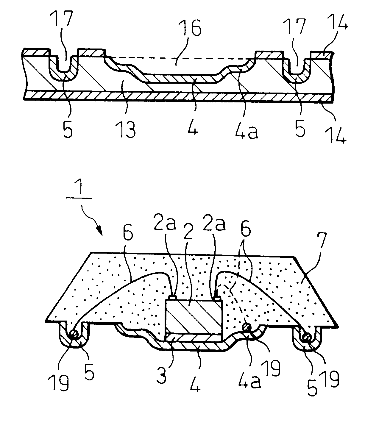
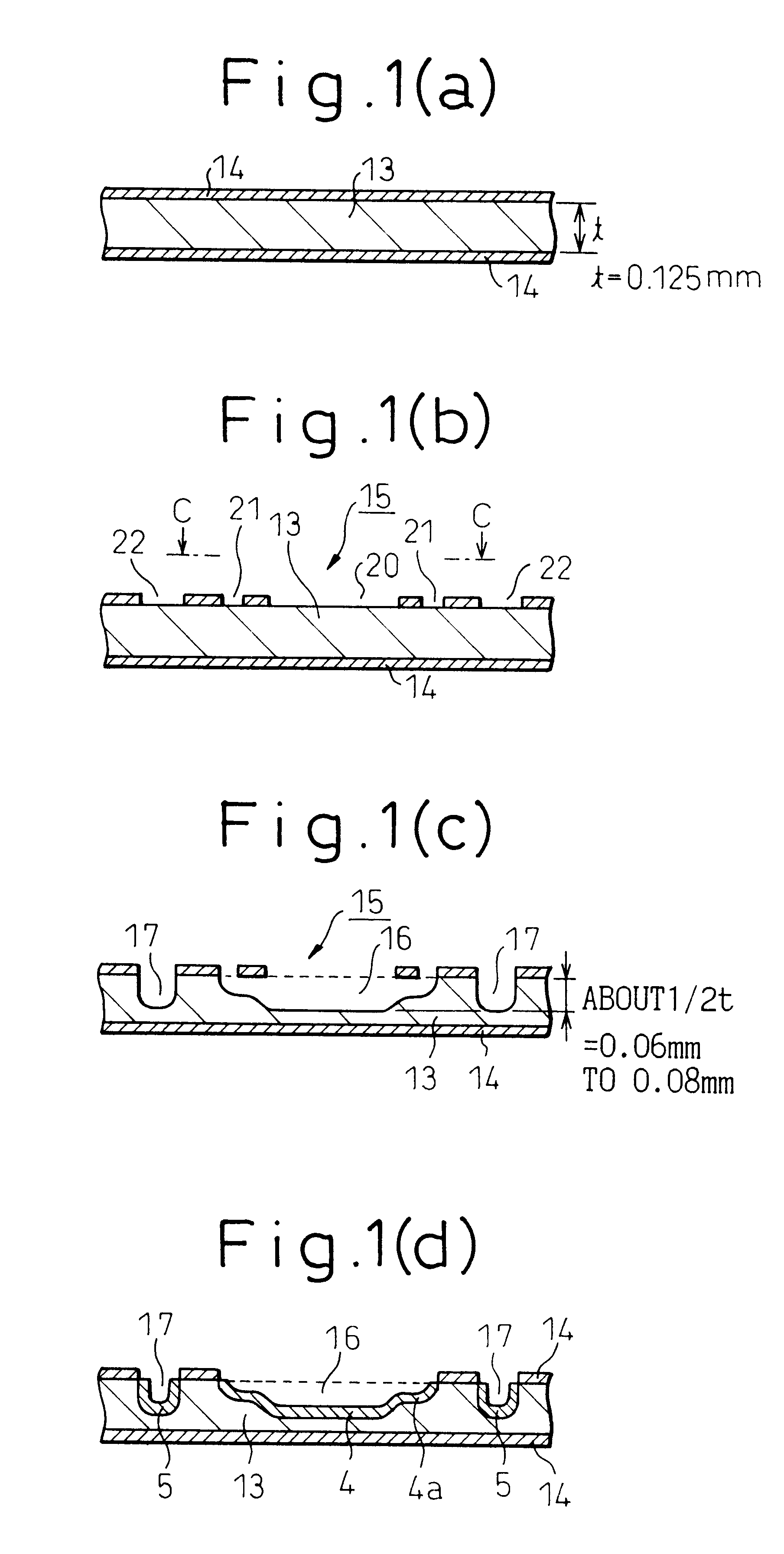
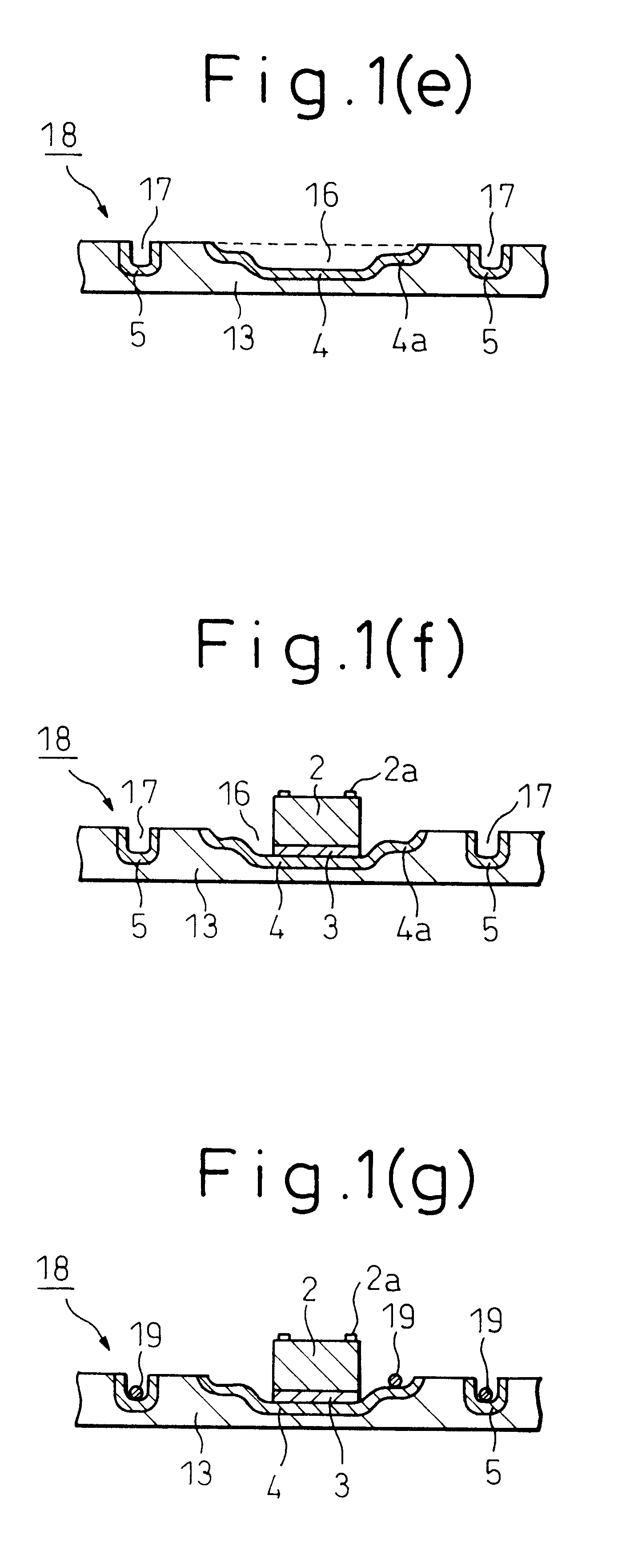
In this embodiment, a description will be made of a semiconductor device carrying a high-frequency analog IC thereon used for an electronic equipment such as a mobile phone and a process for the production thereof. FIGS. 1(a) to 1(j) illustrate a process for producing the semiconductor device; FIG. 2 is a sectional view of one example of a metallic film; and FIG. 3 is a view as seen in the arrowed direction C--C in FIG. 1(b).

Initially, a structure of the semiconductor device will be explained. With reference to FIG. 1(j), reference numeral 1 denotes a semiconductor device having the following structure. A semiconductor chip 2 is mounted onto a bottom of a mounting part metallic film 4 formed in a stepwise configuration via an adhesive layer 3. A material excellent in heat dissipation ability and electro-conductivity, such as an electro-conductive...


PUM


Abstract

A semiconductor device comprises a semiconductor element having a signal electrode and a ground electrode. A mounting part metallic film has a bottom area on which the semiconductor element is mounted and a stepped area located at a periphery of the bottom area and being higher in horizontal level than the bottom area. A connector part metallic film is spaced from the mounting part metallic film and arranged at a peripheral region thereof. The signal electrode of the semiconductor element is electrically connected to the connector part metallic film and the ground electrode of the semiconductor element is electrically connected to the stepped area of the mounting part metallic film. The semiconductor element is shielded with resin together with mounting / connecting sides of the mounting part metallic film and the connector part metallic film.

Description

1. Field of the InventionThe present invention relates to a semiconductor device, a process for producing the same, a carrier substrate and a process for producing the same.2. Description of the Related ArtAs small-sized electronic equipments, such as mobile phones or others, have been come into wide use, there has been a demand for minimizing the size and cutting the production cost of semiconductor devices to be installed in such electronic equipments. A conventional semiconductor device, wherein a semiconductor chip mounted onto a lead frame is resin-shielded, has a problem in that an area extending between inner and outer leads or a mounting area is relatively large. Further, in a BGA (ball grid array) type semiconductor device, there is another problem in that the production cost is high because it necessitates a substrate for mounting a semiconductor chip.To minimize a size of a semiconductor device and to reduce a mounting area therefor, as well as to cut the production cost,...

Claims


Application Information

Patent Timeline
Patent Type & Authority Patents(United States)
IPC IPC(8): H01L21/68H01L23/31H01L23/28H01L21/67H05K3/20H01L23/12H01L21/56H01L23/48H01L23/50
CPCH01L21/568H01L23/3107H01L24/48H01L24/85H01L2224/48228H01L2224/48247H01L2224/48257H01L2224/4848H01L2224/73265H01L2224/83005H01L2224/85005H01L2224/85051H01L2224/92247H01L2924/01004H01L2924/01029H01L2924/01033H01L2924/01046H01L2924/01047H01L2924/01078H01L2924/01079H01L2924/01082H01L2924/014H01L2924/3025H05K3/20H01L2224/48465H01L2224/83001H01L2224/85001H01L2224/32245H01L2924/00H01L2924/01005H01L2924/01006H01L2224/45144H01L2224/48227H01L24/45H01L2224/85205H01L2924/00014H01L2924/181H01L2924/00012H01L2224/85399H01L2224/05599H01L23/48
Inventor FURUHATA, YOSHIOKOBAYASHI, TSUYOSHI
Owner SHINKO ELECTRIC IND CO LTD
Why Eureka
Try Eureka