
Fingerprint-reading system

a fingerprint-reading and fingerprint-reading technology, applied in the field of fingerprint-reading systems, can solve the problems of preventing the use of optical systems, affecting the entry of optical systems into the market, and affecting the accuracy of fingerprint-reading systems,

Inactive Publication Date: 2002-10-01
APPLE INC
View PDF20 Cites 171 Cited by
  • Summary
  • Abstract
  • Description
  • Claims
  • Application Information

AI Technical Summary

Benefits of technology

The system achieves cost-effective and reliable fingerprint authentication by reducing sensor size, stabilizing image quality, and enabling efficient image reconstruction, thereby improving the efficiency and reliability of the authentication process.

Problems solved by technology

However, the optical systems cannot be used to ascertain that the finger that has been placed before the sensor is truly a live finger and is not for example a mold.
The optical systems have other drawbacks such as for example their great volume and high production cost.
These types of sensors, which can be directly integrated into a semiconductor substrate, have drawbacks that hamper their entry into the market.
The efficiency of manufacture of silicon wafers diminishes in proportion to their surface area and thus considerably increases the cost of manufacture.
The quality of contrast of these images is not stable and they tend to fade away.
This complicates the task of the recognition system for it is then necessary to analyze all the images that are being constantly produced by the sensor in order to find the one most appropriate for authentication.
Systems with excitation external to the sensor have been proposed, for example the sending of an energy beam in the form of microwaves, but they complicate the system and increase its volume and cost.
However this complicates the designing of the sensor and increases its cost of manufacture for it requires technology that enables memory storage.
It is very difficult to build a system that is sufficiently precise, reliable and inexpensive, and capable of deciding which is the best image among those produced by the sensor.

Method used


Image

  • Fingerprint-reading system
  • Fingerprint-reading system
  • Fingerprint-reading system

Examples


Embodiment Construction

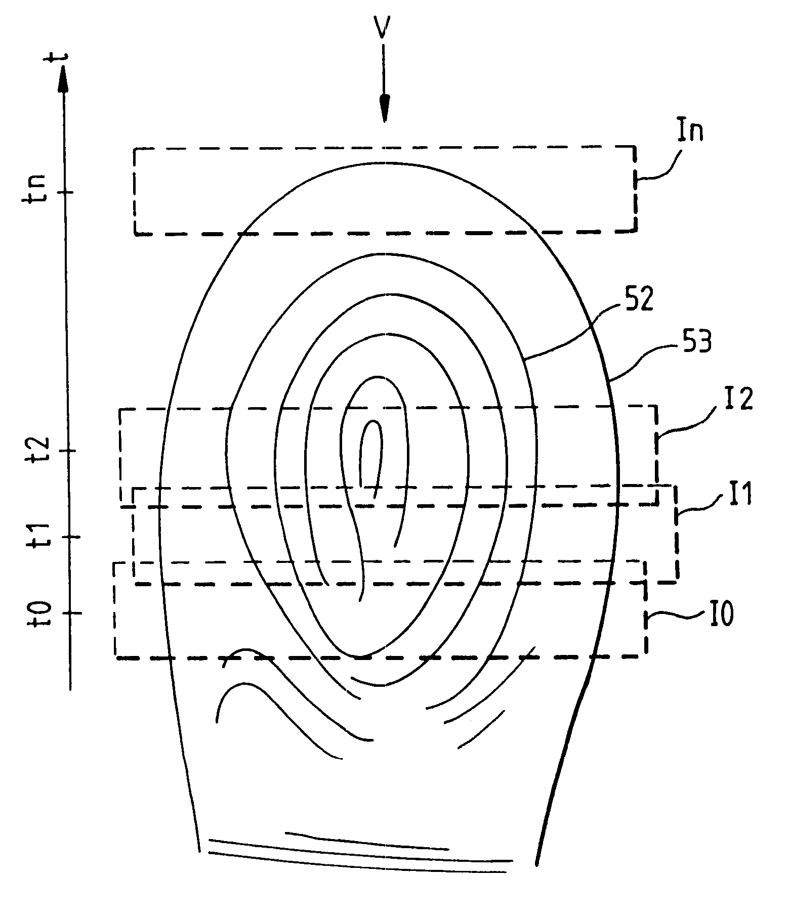
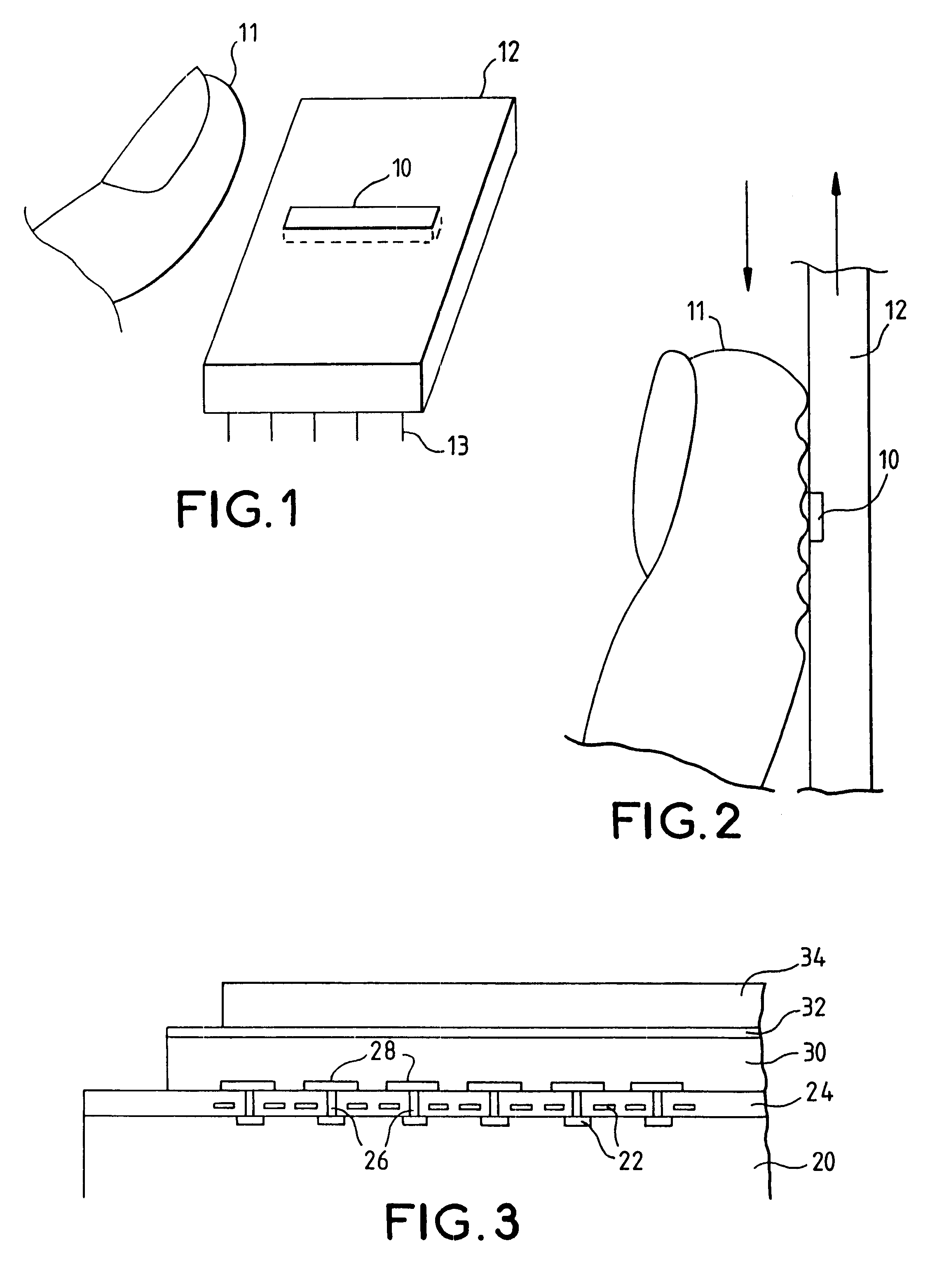
FIG. 1 shows a general view of an exemplary embodiment of a fingerprint sensor according to the invention. The fingerprint sensor 10 is an integrated circuit having the shape of a small bar with a width that substantially equal to that of a finger 11. For example its width is 1 or 2 centimeters. However its length is far smaller than its width. For example its length is some millimeters. The fingerprint sensor 10 partially covers the fingerprint to be read. The sensor is contained in a support 12 comprising external connection pins 13.

In one embodiment, the integrated circuit consists of an active layer of pyroelectric / piezoelectric material placed between an upper electrode and a matrix array of lower electrodes. The lower electrodes lie on a semiconductor substrate in which there is formed an integrated electronic circuit capable of processing the electric charges generated by the pyroelectric / piezoelectric layer on each of the electrodes of the array. This integrated electronic c...


PUM


Abstract

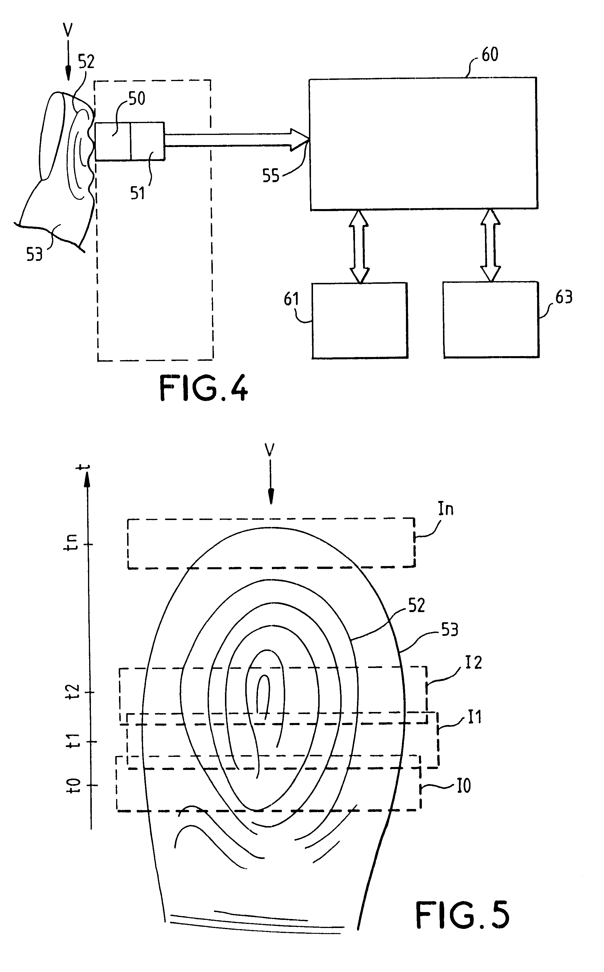
A fingerprint-reading system includes a fingerprint sensor having an active surface sensitive to the pressure and a temperature of a finger. The surface area of this sensor is far smaller than the surface area of the fingerprint to be read. The reading is done when the sensor and the finger are in contact and in a relative motion of sliding of the sensor and the finger with respect to each other. The system reconstitutes a complete image of the fingerprint from the partial images given by the sensor during this motion.

Description

1. Field of the InventionThe invention relates to systems for the reading of fingerprints used especially in devices for authenticating individuals.2. Description of the Prior ArtThe many systems used to authenticate individuals, based on fingerprint analysis, comprise at least one sensor used to obtain an image of the fingerprint of the individual to be identified. In present systems, the finger is placed on the sensor whose reading surface must necessarily have a size of the order of magnitude of the size of the finger. The sensor is associated with a system of analysis used to compare the image of the fingerprint that it gives with an image of a reference fingerprint stored in an adequate medium, for example a chip card.In most cases, the sensors give an analog type of information element and the system of analysis makes use of an operation for the digital processing of the image of the fingerprint which must be digitized at output of the sensor by means of an analog-digital conv...

Claims


Application Information

Patent Timeline
Patent Type & Authority Patents(United States)
IPC IPC(8): G06K9/00G01B7/28G06T1/00G06T7/00
CPCG06K9/00026G06K9/0002G06V40/1335G06V40/1306
Inventor MAINGUET, JEAN-FRAN.CEDILLA.OIS
Owner APPLE INC
Learn More