Cold cathode field emission device and display

a cold cathode field and emission device technology, applied in the manufacture of electrode systems, discharge tubes/lamps, discharge tubes luminescent screens, etc., can solve the problems of large deposition apparatus, difficult to improve a throughput, and non-uniform image display characteristic of display, etc., to achieve uniform and excellent electron emission characteristics

Inactive Publication Date: 2002-10-15
SONY CORP
View PDF13 Cites 25 Cited by
  • Summary
  • Abstract
  • Description
  • Claims
  • Application Information

AI Technical Summary

Benefits of technology

It is therefore an object of the present invention to provide a cold cathode field emission device (to be sometimes referred to as "field emission device" hereinafter) and a process for the production thereof, which can overcome the above production problems in a conventional Spindt type cold cathode field emission device and enables the production of a plurality of cold cathode field emission devices having uniform and excellent electron emitting characteristics by a simple method, and a cold cathode field emission display (to be sometimes referred to as "display" hereinafter) constituted by utilizing the above field emission devices.
In the production process according to each of the second-A to second-D aspects of the present invention, it is particularly preferred to form the second conductive material layer by a CVD method excellent in step coverage (step covering capability) for forming the recess in the surface of the second conductive material layer on the basis of the step between the upper end portion and the bottom portion of the opening portion.

Problems solved by technology

Moreover, the above variability of the distances occurs not only among lots of products but also in one lot of the products, and it causes a non-uniformity in image display characteristic of the display, for example, brightness of an image.
Further, the conductive material layer 205A is generally formed as a layer having a thickness of approximately 1 .mu.m or more, and the formation thereof by a vapor deposition method takes a time period of units of several tens of hours, which involves problems that it is difficult to improve a throughput and that a large deposition apparatus is required.
Further, it is also very difficult to form the peeling-off layer 206 uniformly on the entire surface of a substratum having a large area by an oblique vapor deposition method.
Moreover, not only it is very difficult to peel off the peeling-off layer 206 over the support 200 having a large area for producing a display having a large area, but also the peeling of the peeling-off layer 206 causes contamination and causes the production yield of displays to decrease.
When the thickness of the insulating layer 202 is decreased, however, it is difficult to decrease the capacitance between wiring lines (between the gate electrode 203 and the cathode electrode 201), so that there are caused problems that not only a load on an electric circuit of the display increases but also the display is downgraded in in-plane uniformity and image quality.

Method used


Image

  • Cold cathode field emission device and display
  • Cold cathode field emission device and display
  • Cold cathode field emission device and display

Examples


example 1

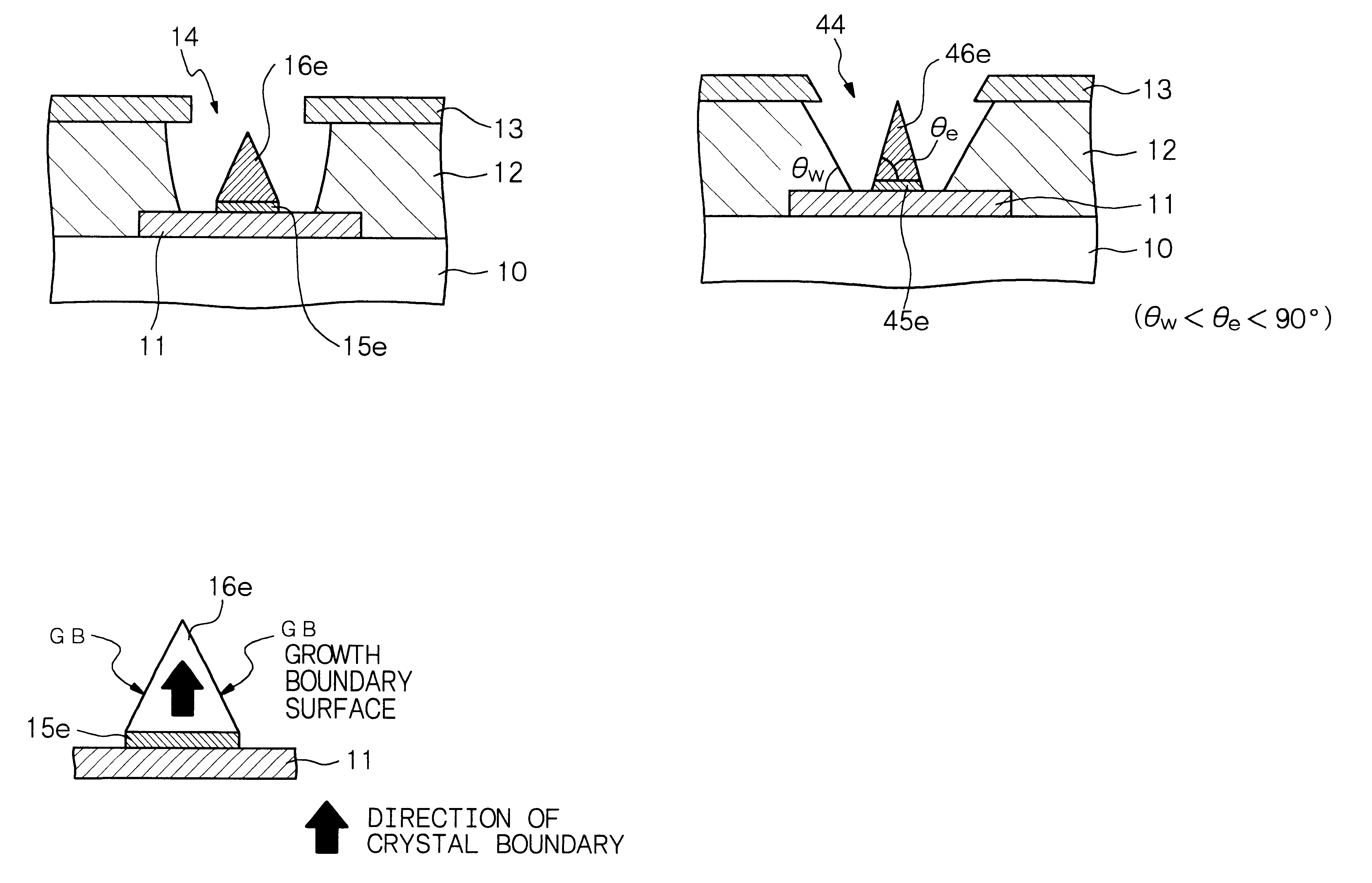
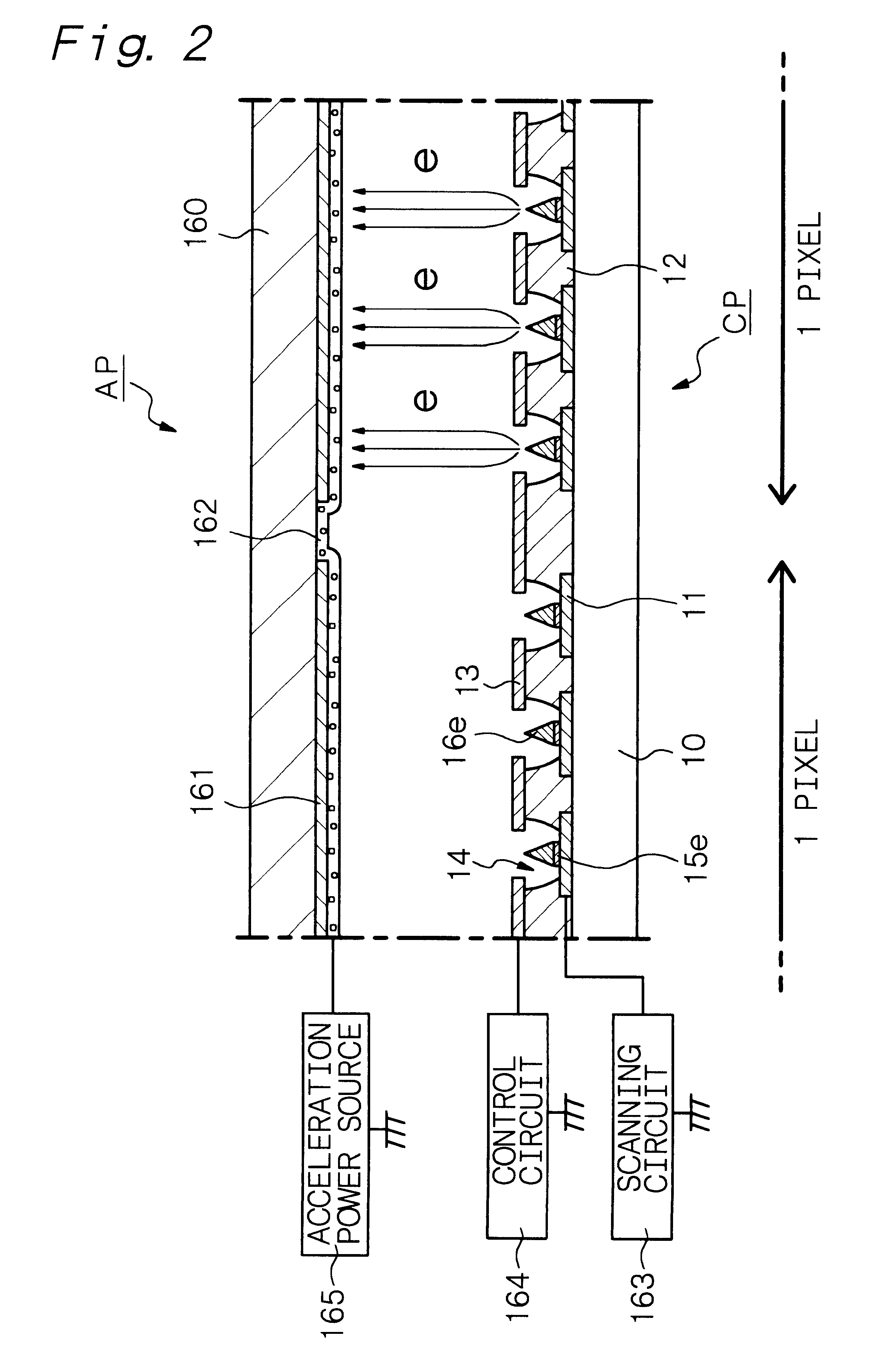
is directed to a field emission device according to the first aspect of the present invention, a display having such field emission devices according to the first aspect of the present invention and a process for the production of a field emission device according to the first-A aspect of the present invention. FIG. 1A shows a schematic partial end view of the field emission device of Example 1, and particularly, FIG. 1B schematically shows an electron emitting portion and members in its vicinity. FIG. 2 shows a schematic partial end view of the display, and further, FIGS. 3A, 3B, 4A, 4B, 5A, 5B, 6A, 6B, 7A, 7B and 7C show the process for the production of the field emission device.

The field emission device comprises a support 10 formed, for example, of a glass substrate, a cathode electrode 11 composed of chromium (Cr), an insulating layer 12 composed of SiO.sub.2, a gate electrode 13 composed of chromium and a conical electron emitting portion 16e formed of a tungsten (W) layer. T...

example 2

Example 2 is directed to the process for the production of a field emission device according to the first-B aspect of the present invention. FIGS. 8A, 8B, 9A, 9B, 10A, 10B, 11A and 11B show the production process of Example 2. Those portions which are the same as those in FIGS. 1A and 1B are shown by the same reference numerals, and detailed explanations thereof are omitted.

[Step-200]

First, the cathode electrode 11 is formed on the support 10. The cathode electrode 11 is formed by subsequently forming a TiN layer (thickness 0.1 .mu.m), a Ti layer (thickness 5 nm), an Al--Cu layer (thickness 0.4 .mu.m), a Ti layer (thickness 5 nm), a TiN layer (thickness 0.02 .mu.m and a Ti layer (thickness 0.02 .mu.m) in this order by a DC sputtering method, for example, according to a sputtering condition shown in the following Table 10 to form laminated layers and patterning the laminated layers. In the drawings, the cathode electrode 11 is shown as a single layer. Then, the insulating layer 12 is...

example 3

Example 3 is directed to the process for the production of a field emission device according to the first-C aspect of the present invention. The production process of Example 3 will be explained with reference to FIGS. 12A, 12B and 13. Those portions which are the same as those in FIGS. 8A, 8B, 9A, 9B, 10A and 10B are shown by the same reference numerals, and detailed explanations thereof are omitted.

[Step-300]

Procedures up to the formation of the mask material layer 27 are carried out in the same manner as in [Step-200] to [Step-220] in Example 2. Then, the mask material layer 27 only on the conductive material layer 26 and in the widened portion 26C is removed to leave the mask material layer 27 in the columnar portion 26B as shown in FIG. 12A. In this case, wet etching using a diluted hydrofluoric acid aqueous solution is carried out, whereby only the mask material layer 27 composed of copper can be selectively removed without removing the conductive material layer 26 composed of...


PUM


Abstract

A cold cathode field emission device comprising; (A) a cathode electrode formed on a support, (B) an insulating layer formed on the support and the cathode electrode, (C) a gate electrode formed on the insulating layer, (D) an opening portion which penetrates through the gate electrode and the insulating layer, and (E) an electron emitting portion which is positioned at a bottom portion of the opening portion and has a tip portion having a conical form and being composed of a crystalline conductive material, the tip portion of the electron emitting portion having a crystal boundary nearly perpendicular to the cathode electrode.

Description

BACKGROUND OF THE INVENTION AND RELATED ART STATEMENTThe present invention relates to a cold cathode field emission device, a process for the production thereof and a cold cathode field emission display. More specifically, it relates to a cold cathode field emission device of which the tip portion has a conical form, a process for the production thereof and a flat panel type cold cathode field emission display having the above cold cathode field emission devices arranged in a two-dimensional matrix form.Various flat panel type displays are studied for substitutes for currently main-stream cathode ray tubes (CRT). The flat type displays include a liquid crystal display (LCD), an electroluminescence display (ELD) and a plasma display (PDP). Further, a cold cathode field emission type display which can emit electrons from a solid into vacuum without relying on thermal excitation, that is, a so-called field emission display (FED) is proposed as well, and it attracts attention from the v...

Claims


Application Information

Patent Timeline
Patent Type & Authority Patents(United States)
IPC IPC(8): H01J9/02H01J1/30
CPCH01J9/025H01J2329/00H01J1/30
Inventor KUBOTA, SHINJIKIKUCHI, KAZUOSATA, HIROSHI
Owner SONY CORP
Why Eureka
Try Eureka