Method and apparatus for measuring thickness variation of a thin sheet material, and probe reflector used in the apparatus

a thin sheet material and thickness variation technology, applied in the direction of measuring devices, instruments, using optical means, etc., can solve the problems of deterioration of surface, limiting measurement precision of above described apparatus, and crucial above problems

Inactive Publication Date: 2002-11-12
PANASONIC CORP
View PDF6 Cites 39 Cited by
  • Summary
  • Abstract
  • Description
  • Claims
  • Application Information

AI Technical Summary

Problems solved by technology

Deterioration in surface planarity may blur the patterns of semiconductor elements or circuits formed by photoetching, or make the contour of a material printed in patterns on the wafer surface unclear.
With the increase in density and scale of semiconductor elements and circuits, the above problem becomes crucial.
However, the above described apparatus has a limit to measurement precision, and is not suitable for highly precise thickness variation measurement required for the fabrication of semiconductor devices of high density in recent years.
Measurement precision of wafer thickness variation by this capacitance sensor is thus apt to deteriorate.
Further, precise measurement of capacitance at the peripheral edge of the wafer is practically impossible, and since the thickness variation in this part cannot be estimated, it is normally regarded that such peripheral portion of the wafer to a width of about 3 mm from the outermost edge of the wafer cannot be used for semiconductor devices.
Wafer material is accordingly wasted.
Moreover, in some cases depending on conductive properties of the wafer, measurement by the above capacitance displacement sensor is technically difficult.
Also, as noted above, measurement results are greatly affected by ambient conditions between the sensor and the wafer.
Theoretically, such high precision in thickness variation measurement can hardly be achieved with the above described capacitance displacement sensor, which is said to have the precision of about 0.05 .mu.m.

Method used


Image

  • Method and apparatus for measuring thickness variation of a thin sheet material, and probe reflector used in the apparatus
  • Method and apparatus for measuring thickness variation of a thin sheet material, and probe reflector used in the apparatus
  • Method and apparatus for measuring thickness variation of a thin sheet material, and probe reflector used in the apparatus

Examples


Embodiment Construction

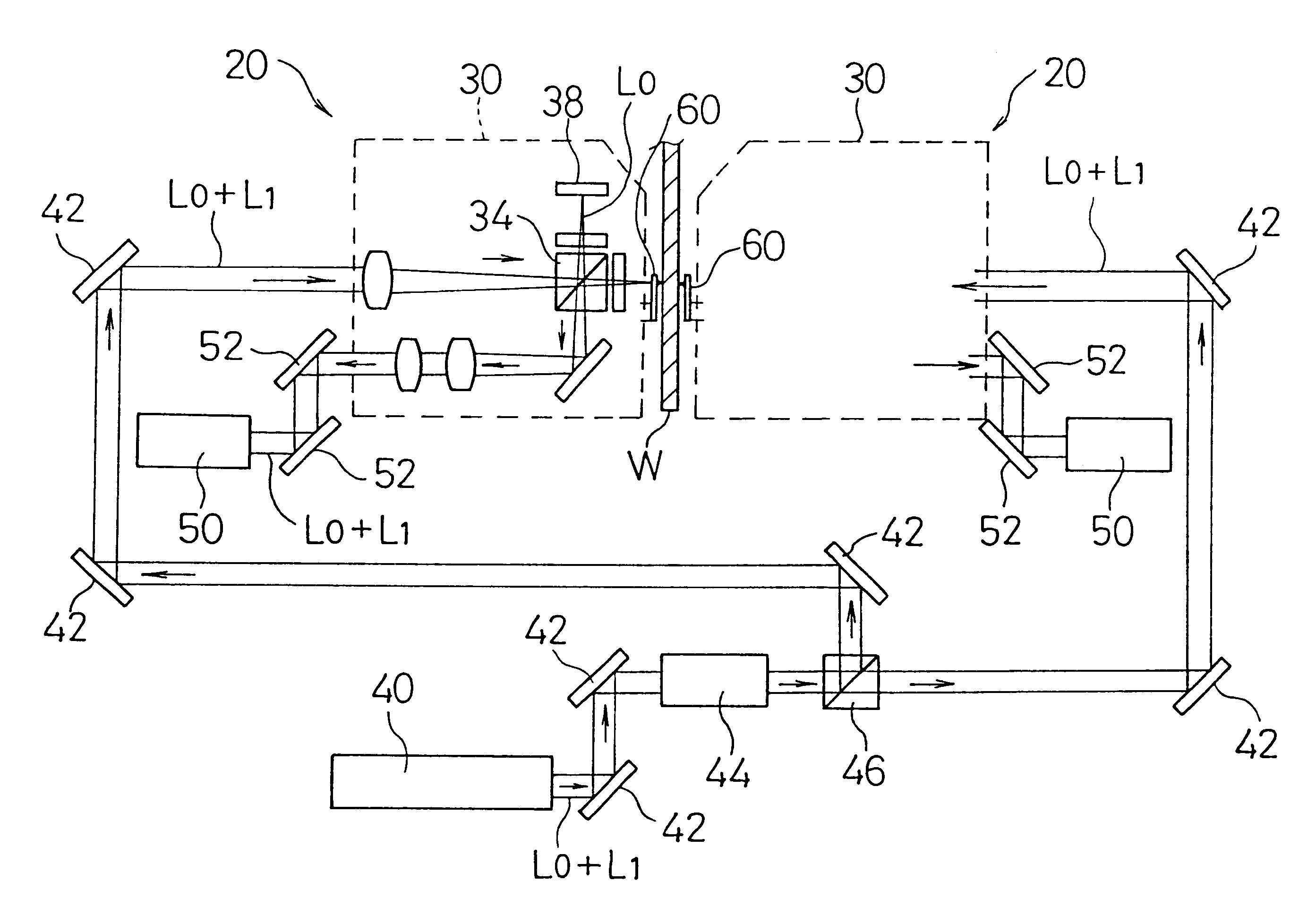
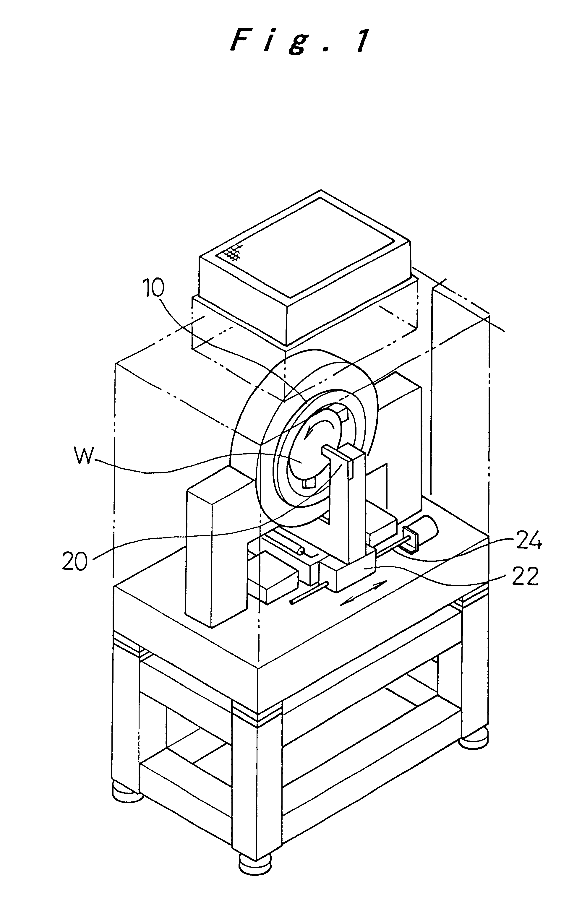
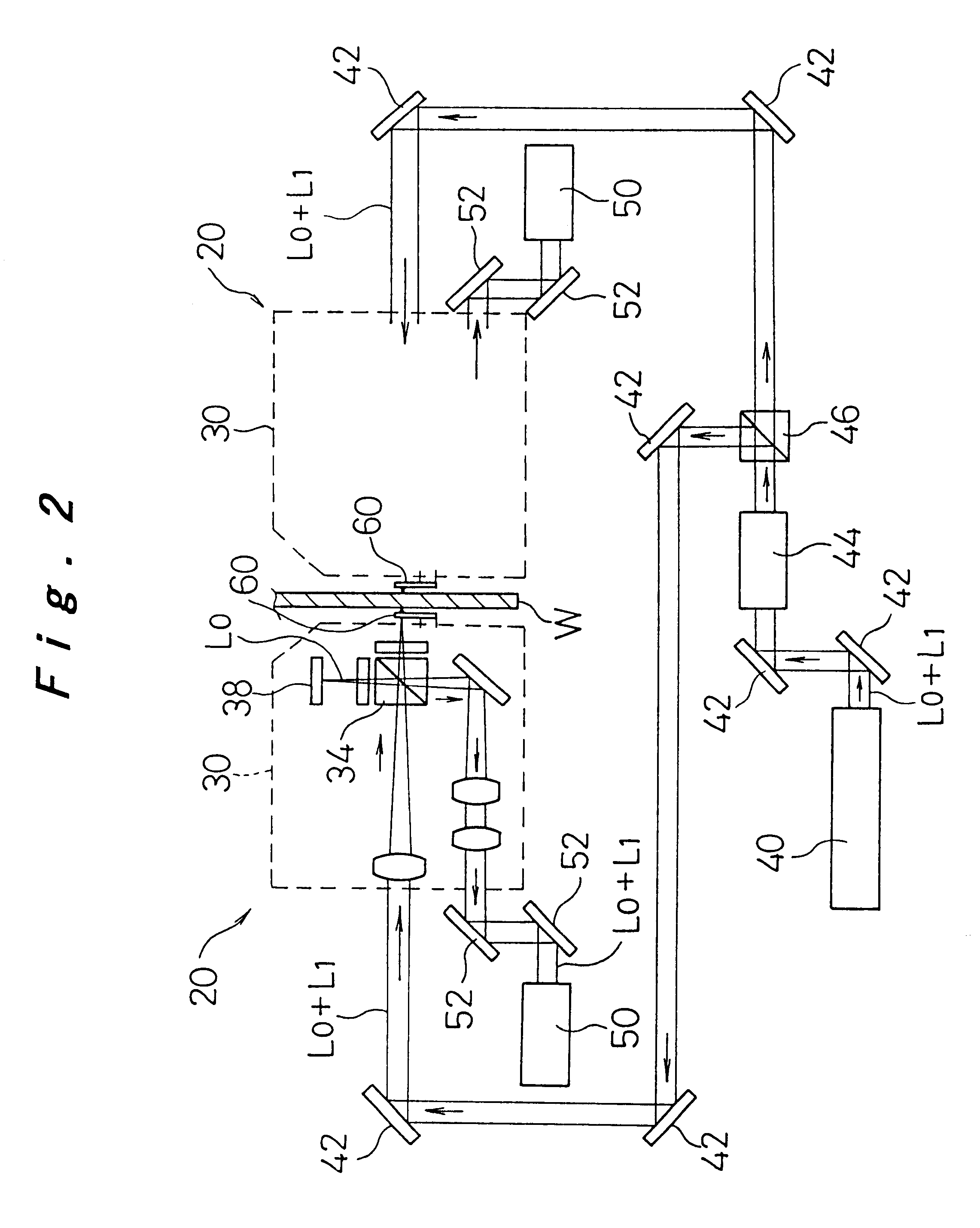
FIG. 1 shows the entire construction of the thickness variation measuring apparatus for semiconductor wafers according to one embodiment of the present invention. A wafer w is held vertically upright by a circular hollow spindle 10, and is rotated within the vertical plane by rotation of the hollow spindle 10. To one side opposite both faces of the wafer w, a pair of optical displacement gauges 20 are respectively disposed. Although only the one on the side of the front surface is shown in the drawing, the optical displacement gauge 20 is also arranged on the backside opposite the one on the front surface. The pair of optical displacement gauges 20 are mounted such as to be movable in a direction parallel to the surface of the wafer w, so that the measurement position of the optical displacement gauges 20 moves leftwards and rightwards along the radius of the wafer w. Specifically, the optical displacement gauges 20 are mounted on a table 24 that is linearly moved on a ball screw 24...


PUM

PropertyMeasurementUnit
widthaaaaaaaaaa
thicknessaaaaaaaaaa
speedaaaaaaaaaa

Abstract

Optical displacement gauges 20 are respectively arranged on both sides of a thin sheet material w, and displacement of surface position of the thin sheet material w is measured by irradiating measurement light L1 to the surface of the thin sheet material w. Thickness variation of the thin sheet material w is obtained from the measurement results of displacement of the surface position of the thin sheet material w.

Description

1. Technical Field of the InventionThe present invention relates to a method and apparatus for measuring thickness variation of a thin sheet material. More particularly, the present invention relates to measurement of thickness variation of wafers for use in semiconductor devices, which need to meet stringent requirements for little variation in thickness in a surface direction, and further relates to a probe reflector used in the thickness variation measuring apparatus.2. Description of Related ArtWafers used for semiconductor devices consist of a thin sheet material of silicone or the like. For fabrication of semiconductor elements and circuits on the surface of a wafer, photoetching techniques, printing techniques, and various micro machining techniques are applied.In processing a wafer using these techniques, it is essential to achieve high planarity of the wafer surface. Deterioration in surface planarity may blur the patterns of semiconductor elements or circuits formed by pho...

Claims


Application Information

Patent Timeline
Patent Type & Authority Patents(United States)
IPC IPC(8): G01B11/06G01B11/30G01B21/08G01B21/30
CPCG01B11/06G01B11/306G01B21/08G01B21/30
Inventor KUBO, KEISHIYOSHIZUMI, KEIICHIIMADA, YUKIOTAKEUCHI, HIROYUKIHANDA, KOJI
Owner PANASONIC CORP
Why Eureka
Try Eureka