Method for manufacturing a semiconductor device

a manufacturing method and semiconductor technology, applied in semiconductor devices, semiconductor/solid-state device details, electrical devices, etc., can solve the problems of resin peeling away from the interface with the wafer, lower sealing reliability relative to a conventional package, etc., to improve the sealing reliability of resin, improve the yield of mounting surfaces, and improve the effect of precision

Inactive Publication Date: 2002-11-19
TEXAS INSTR INC
View PDF5 Cites 67 Cited by
  • Summary
  • Abstract
  • Description
  • Claims
  • Application Information

AI Technical Summary

Benefits of technology

An objective of the present invention is to provide a manufacturing method that improves the resin sealing reliability in a wafer-level CSP semiconductor device.
Another objective of the prese

Problems solved by technology

However, in this type of semiconductor device, the resin does not cover the sides of the semiconductor chips so the sealing reliability is lower relative to a conventional pa

Method used


Image

  • Method for manufacturing a semiconductor device
  • Method for manufacturing a semiconductor device
  • Method for manufacturing a semiconductor device

Examples


Embodiment Construction

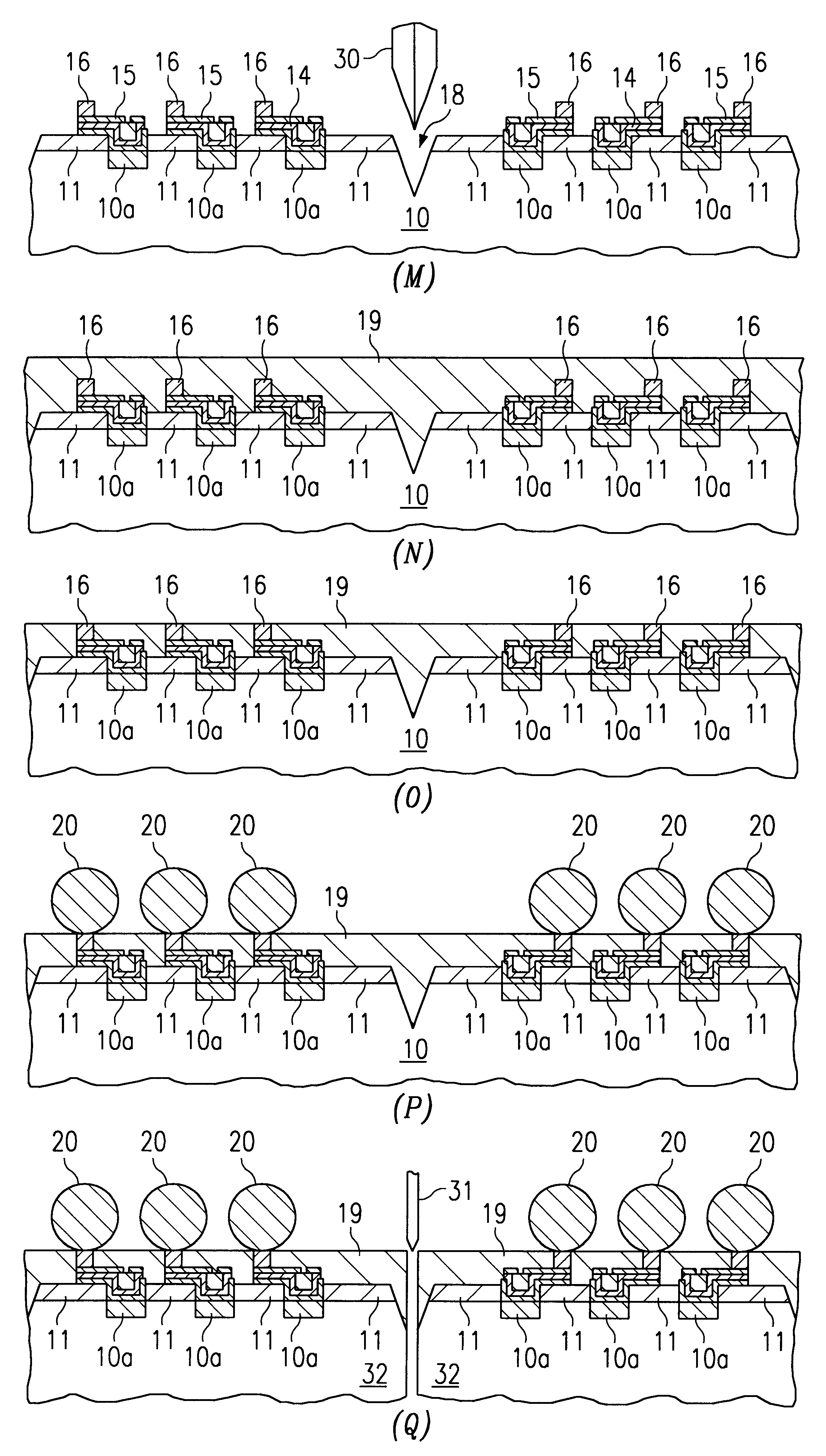
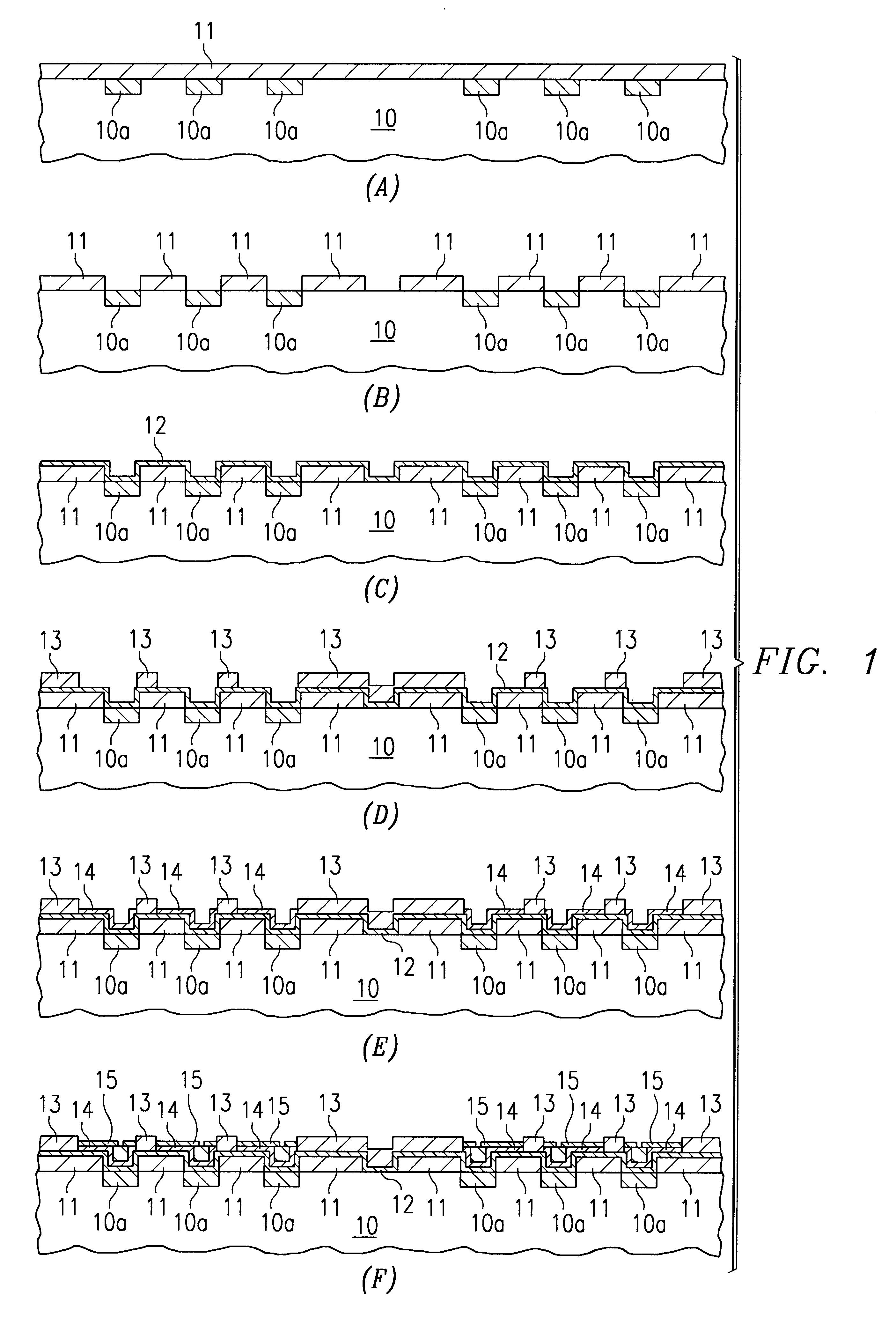
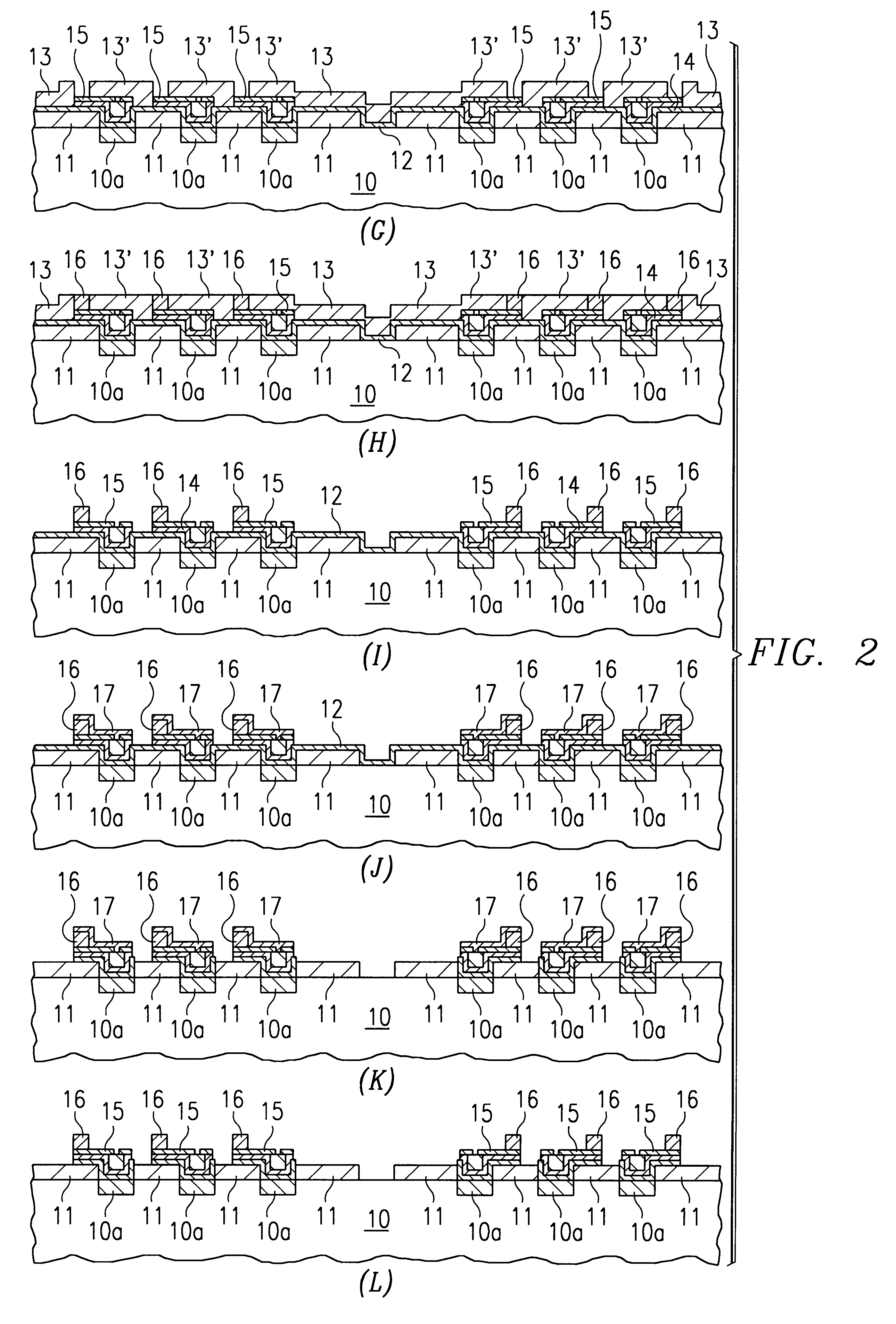
Next, an embodiment of the present invention is explained with reference to the figures. In the method for manufacturing a semiconductor device of this embodiment, a package is processed as a wafer on which semiconductor elements are formed, and a packaged semiconductor device is finally obtained at the stage where the wafer is diced. The manufacturing method of this embodiment includes a process that forms required wiring on the wafer surface on which the semiconductor elements are formed, a process that forms conductive supports, a process that forms a groove along the boundary lines of the semiconductor elements, a process that seals the wafer surface with a resin, a process that applies solder balls which are used as external terminals, and a process that produces each package by dicing the wafer. These detailed processes are sequentially illustrated in FIGS. 1-3. Also, someone skilled in the art should recognize that these figures are not to scale. Also, in the figures, only a ...


PUM


Abstract

A method to improve the resin sealing reliability in the manufacturing of a wafer-level CSP. The method for manufacturing a semiconductor device of the present invention includes a process that forms wiring 14 and conductive supports 16, which electrically connect electrode pads 10a and corresponding external terminals, on a wafer 10 on which semiconductor elements are formed. In subsequent processes, a groove 18 (preferably V shaped) is formed in the surface of the above-mentioned wafer along the boundary lines of the respective semiconductor elements. Next, the end surfaces of the above-mentioned conductive supports 16 are exposed, and the above-mentioned wafer surface is covered with a resin 19 so that external terminals 20 are arranged on the end surfaces of the conductive supports. In the final process, along the boundary lines of the above-mentioned semiconductor elements, packaged semiconductor devices 32 are obtained by dicing the above-mentioned wafer.

Description

FIELD OF THE INVENTIONThe present invention pertains to a method for manufacturing a semiconductor device. In particular, it pertains to a method for manufacturing a semiconductor device that can package semiconductor chips in a wafer state.BACKGROUND OF THE INVENTIONIn the manufacturing field of semiconductor devices, there is an ongoing effort to further miniaturize a single packaged semiconductor device. The initial effort to miniaturize semiconductor devices involved the reduction of the dimensions of the semiconductor chips themselves. With the reduction of semiconductor chips, the number of chips, which can be obtained from one wafer is increased, and the manufacturing cost is reduced. At the same time,, since the distance required by the electrons to move between the respective elements can be shortened, the operating speed of the device can be increased. With the development of fine machining technologies, the chip size of semiconductor devices with equivalent functions can ...

Claims


Application Information

Patent Timeline
IPC IPC(8): H01L21/02H01L21/60H01L23/485H01L21/768H01L23/31H01L21/70H01L23/28H01L23/48H01L21/78H01L21/301H01L23/02H01L29/06
CPCH01L21/78H01L23/3114H01L24/11H01L24/12H01L24/94H01L2224/94H01L29/0657H01L2224/0231H01L2224/13099H01L2924/01004H01L2924/01015H01L2924/01022H01L2924/01027H01L2924/01029H01L2924/01046H01L2924/01074H01L2924/01078H01L2924/01079H01L2924/01005H01L2924/01006H01L2924/01019H01L2924/01023H01L2924/01024H01L2924/01033H01L2924/014H01L2224/0401H01L2224/11334H01L2224/11H01L2224/05144H01L2224/05147H01L2224/05155H01L2224/05164H01L2224/05166H01L2224/05171H01L2224/05647H01L2224/02311H01L2224/02313H01L2224/02331H01L24/13H01L24/05H01L24/03H01L2924/0001H01L2224/05008H01L2224/05569H01L2224/13024H01L24/02H01L23/02
Inventor MASUMOTO, MUTSUMIMASUMOTO, KENJI
Owner TEXAS INSTR INC
Why Eureka
Try Eureka