Semiconductor physical quantity sensor

a technology of physical quantity and sensor, which is applied in the direction of turn-sensitive devices, instruments, force measurement, etc., can solve the problems of sensor not working normally, and the protrusion in the prior arts not working sufficiently

Inactive Publication Date: 2002-12-17
DENSO CORP
View PDF6 Cites 96 Cited by
  • Summary
  • Abstract
  • Description
  • Claims
  • Application Information

AI Technical Summary

Benefits of technology

is to prevent an adhesion of a movable electrode to a fixed electrode due to an electrostatic attracting force even in a non-detection interval interposed therebetween when the non-detection interval is larger than a detection interval interposed between the movable electrode and an opposite fixed electrode.
Preferably, the protrusions on the both side faces of the first fixed electrode are formed in the same size and the same shape. It may allow stable forming of the protrusions. More preferably, the protrusions on the both sides are disposed symmetrically with respect to a longitudinal direction of the first fixed electrode.

Problems solved by technology

Consequently, the sensor doesn't work normally.
However, the protrusions in the prior arts don't work sufficiently due to the following reason.

Method used


Image

  • Semiconductor physical quantity sensor
  • Semiconductor physical quantity sensor
  • Semiconductor physical quantity sensor

Examples


first embodiment

(First Embodiment)

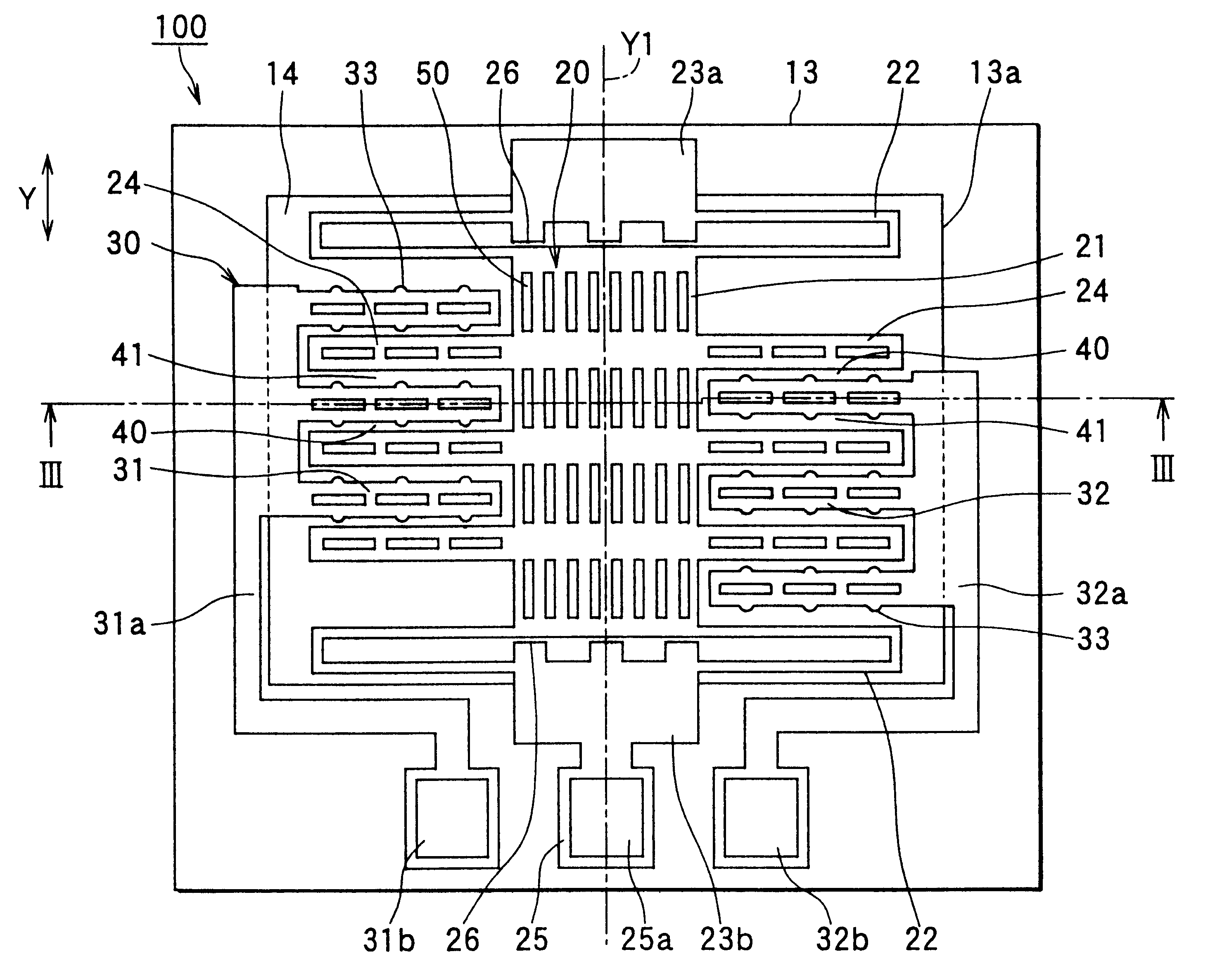
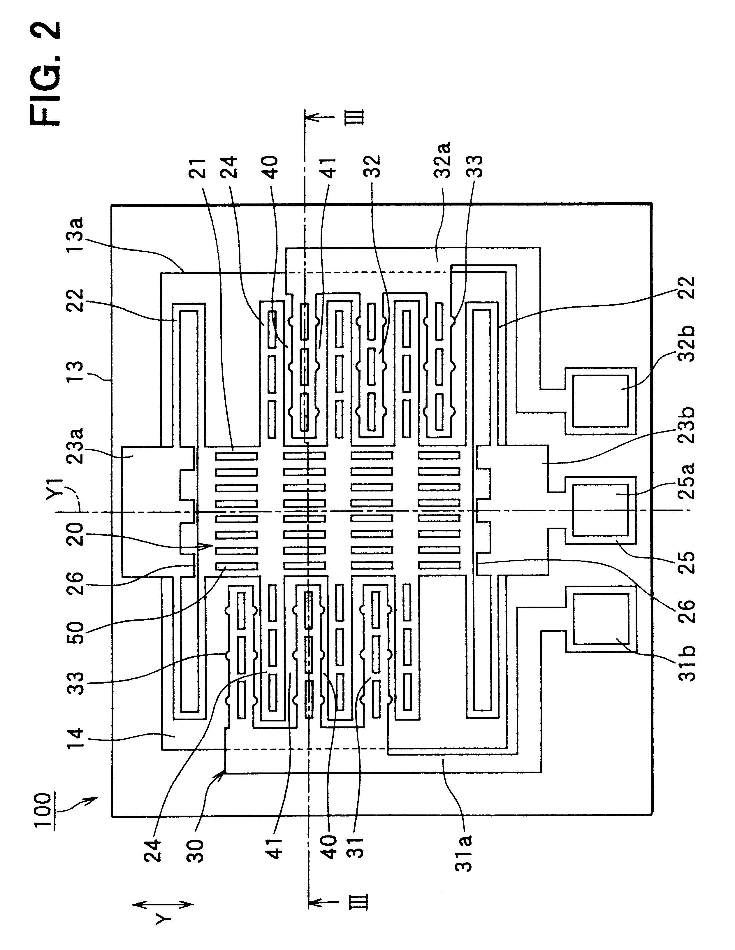
Referring to FIGS. 2 and 3, a semiconductor acceleration sensor 100 (which is simply referred to as a sensor 100 hereinafter) is formed as a rectangular sensor chip in a semiconductor substrate by a well-known micro-machined method. As shown in FIG. 3, the semiconductor substrate forming the sensor 100 is a SOI (Silicon On Insulator) substrate 10 which includes a first silicon substrate (supporting substrate) 11 as a first semiconductor layer, a second silicon substrate 12 as a second semiconductor layer, and an oxide layer 13 as a insulator layer interposed between the first silicon substrate 11 and the second silicon substrate 12.

A beam structure consisting of a movable portion 20 and fixed portion 30 is formed in the second silicon substrate 12. The movable portion 20 is separated from the fixed portion 30 by forming trenches 14. A part of the oxide layer 13 is removed under the beam structure by sacrificial layer etching to make a rectangular opening 13a as sho...

second embodiment

(Second Embodiment)

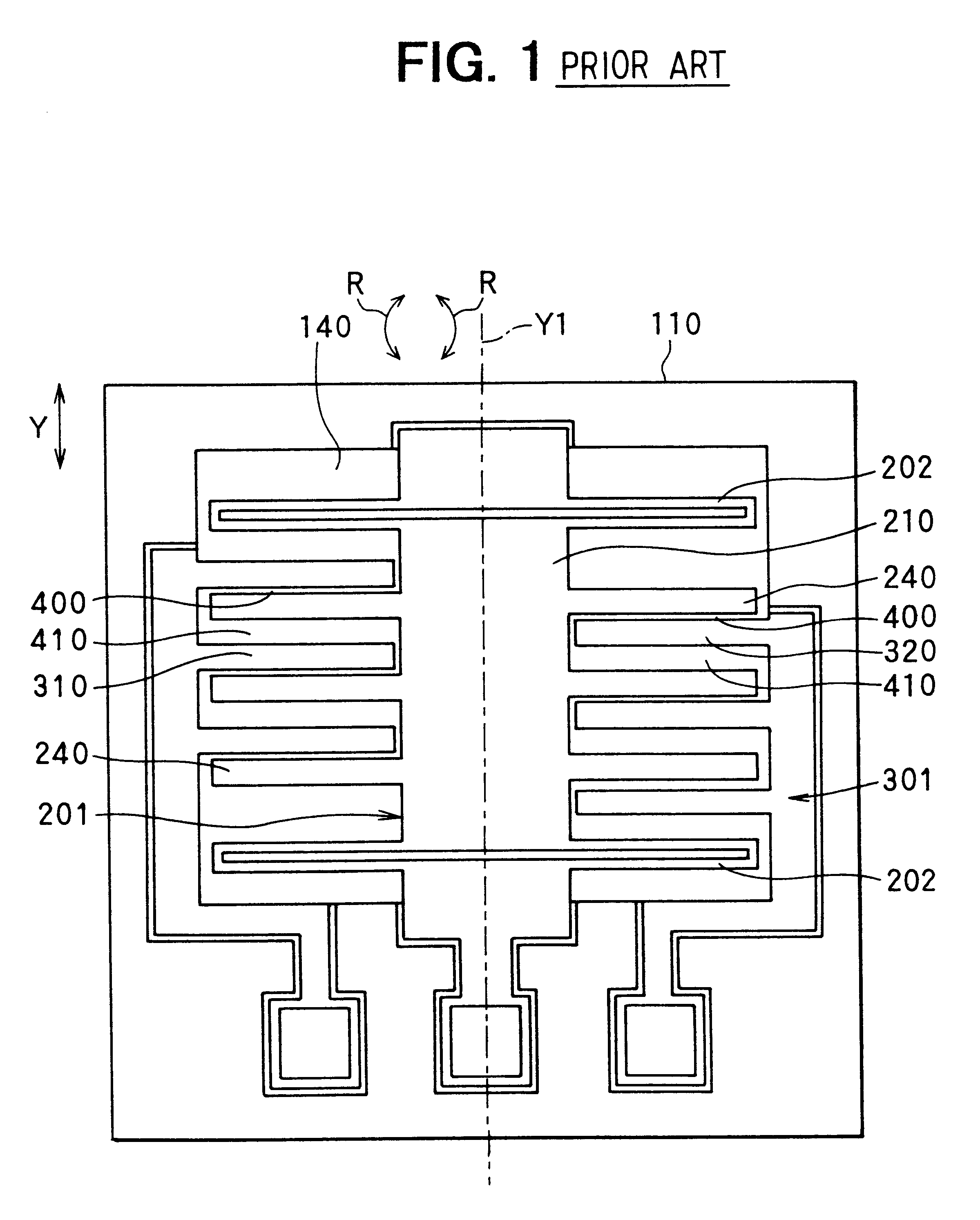
Miniaturization is required for a semiconductor physical quantity detection sensor such as the sensor described in Prior Art and the sensor 100 described above.

For this purpose, it is a useful way to shorten the suspension members 22 in its longitudinal direction in the sensor in FIG. 2. However, the length of the suspension portion is very important because it is main factor of spring modulus that contributes to a sensitivity of the sensor. Therefore, it is not so easy to shorten the length of the suspension members 22.

To solve the new problem described above, it is conceivable to connect several rectangle frame spring portions, each of which is formed with one pair of the suspension members 22, in series in a direction along the axis Y1. In the direction corresponding to the axis Y1, the number of folding times of each rectangle frame spring portion is only one. Therefore, if two rectangle frame spring portions are connected in series, two folds are disposed in ...

third embodiment

(Third Embodiment)

Referring to FIG. 12, a sensor 400 in this embodiment is the same as the sensor 300 in the second embodiment except that the protrusions 33 are not formed on the fixed electrodes 31 and 32 in the sensor 400.

A sensor 400 has a movable portion 20 and a fixed portion 30 on a first silicon substrate 11 (supporting substrate). The movable portion 20 has a weight portion 21 that is movable along a displacement direction Y due to an acceleration applied to the sensor, and comb-shaped movable electrodes 24 formed on both side surfaces of the weight portion 21 centering an axis Y1 in accordance with a displacement direction. The fixed portion 30 has fixed electrodes 31 and 32 each electrode members of which engaging with each of the movable electrodes 24 so as to oppose to the movable electrodes 24. This sensor 400 detects an acceleration applied to the sensor in the displacement direction Y based on a change of capacitance provided with the movable electrodes 24 and the fi...


PUM

PropertyMeasurementUnit
lengthaaaaaaaaaa
lengthaaaaaaaaaa
lengthaaaaaaaaaa

Abstract

A semiconductor acceleration sensor, which prevents an adhesion of a movable electrode to a first or second fixed electrode due to an electrostatic attracting force generated therebetween. The sensor has a weight portion and movable electrodes formed on both sides of which, and first and second fixed electrodes each engaging with the each of the movable electrodes. Each of the first and second fixed electrodes is disposed in parallel with each of the movable electrodes so that side faces thereof determine a detection interval and non-detection interval larger than the detection interval with side faces of adjoining two of the movable electrodes. Protrusions are formed on both of the side faces of each of the first and second fixed electrodes. These protrusions prevent the movable electrodes from adhering to the first or second fixed electrode in both of the detection interval and non-detection interval.

Description

This application is based upon Japanese Patent Application Nos. 2000-79352 filed on Mar. 16, 2000, and 2000-382422 filed on Dec. 15, 2000, the contents of which are incorporated herein by reference.1. Field of the InventionThis invention relates to semiconductor physical quantity sensors for detecting a physical quantity such as acceleration or angular velocity, especially, to a capacitance-detecting type semiconductor physical quantity sensor.2. Related ArtsA structure of a differential capacitance type semiconductor acceleration sensor of a prior art is shown in FIG. 1. A semiconductor layer of a supporting substrate 110 has a moving portion 201 and a fixed portion 301 separated from the moving portion 201 by a trench 140 formed by etching.The moving portion 201 has suspension parts 202 fixed to the supporting substrate 110, a weight portion 210 supported by the suspension parts 202, and two sets of plural movable electrode members 240 connected to both sides of the weight portion...

Claims


Application Information

Patent Timeline
Patent Type & Authority Patents(United States)
IPC IPC(8): B81B3/00G01P15/125G01L1/14G01C19/56G01C19/5733H01L29/84
CPCB81B3/0008G01P15/125B81B2201/0235G01P2015/0814
Inventor SAKAI, MINEKAZUMURATA, MINORU
Owner DENSO CORP
Why Eureka
Try Eureka