Bi-level multilayered microelectronic device package with an integral window

Inactive Publication Date: 2002-12-17
NAT TECH & ENG SOLUTIONS OF SANDIA LLC
View PDF1 Cites 131 Cited by
  • Summary
  • Abstract
  • Description
  • Claims
  • Application Information

AI Technical Summary

Benefits of technology

What is needed is a packaging process that minimizes the number of times that a MEMS device is handled and exposed to temperature cycles and different environments, which can possibly lead to contamination of the device. This can be accomplished by performing as many of the package fabrication steps as possible before mounting the MEMS device. What is needed, then, is a packaging process

Problems solved by technology

Unfortunately, adding windows to these packages typically increases the complexity and costs.
Although stronger, ceramic packages are typically heavier, bulkier, and more expensive to fabricate than plastic molded packages.
Problems with using wirebonding include the fragility of very thin wires; wire sweep detachment and breakage during transfer molding; additional space required to accommodate the arched wire shape and toolpath motion of the wirebond toolhead; and the constraint that the window (or cover lid) be attached after the wirebonding step.
Also, attachment of the window as the last step can limit the temperature of bonding the window to the package.
Problems with this approach include the use of fragile wirebonded interconnections; and plastic encapsulation, which does not provide hermetic sealing

Method used


Image

  • Bi-level multilayered microelectronic device package with an integral window
  • Bi-level multilayered microelectronic device package with an integral window
  • Bi-level multilayered microelectronic device package with an integral window

Examples


Embodiment Construction

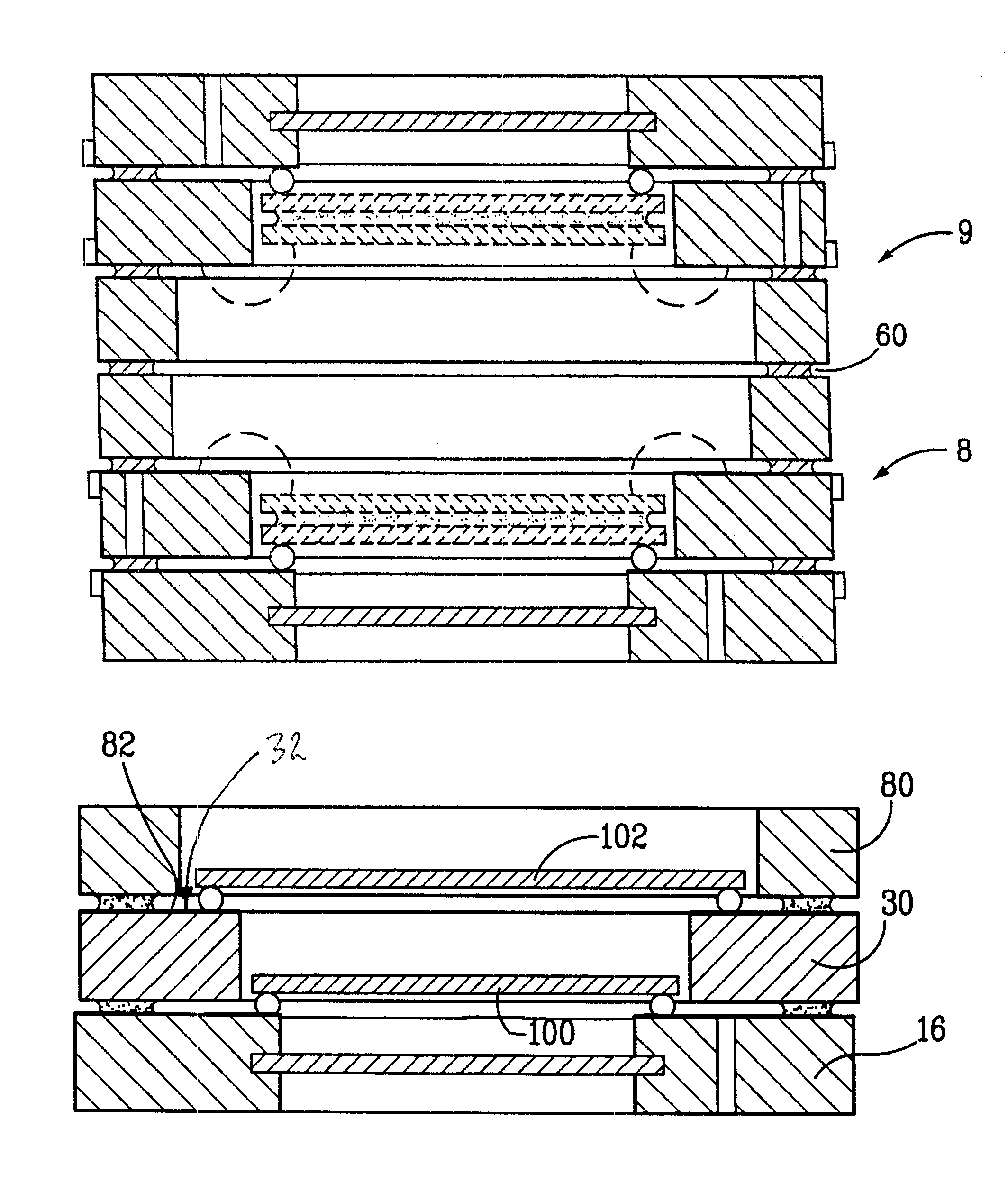
The present invention relates to a package for housing at least one microelectronic device, comprising a hollow assembly of stacked, electrically insulating plates and an integral window.

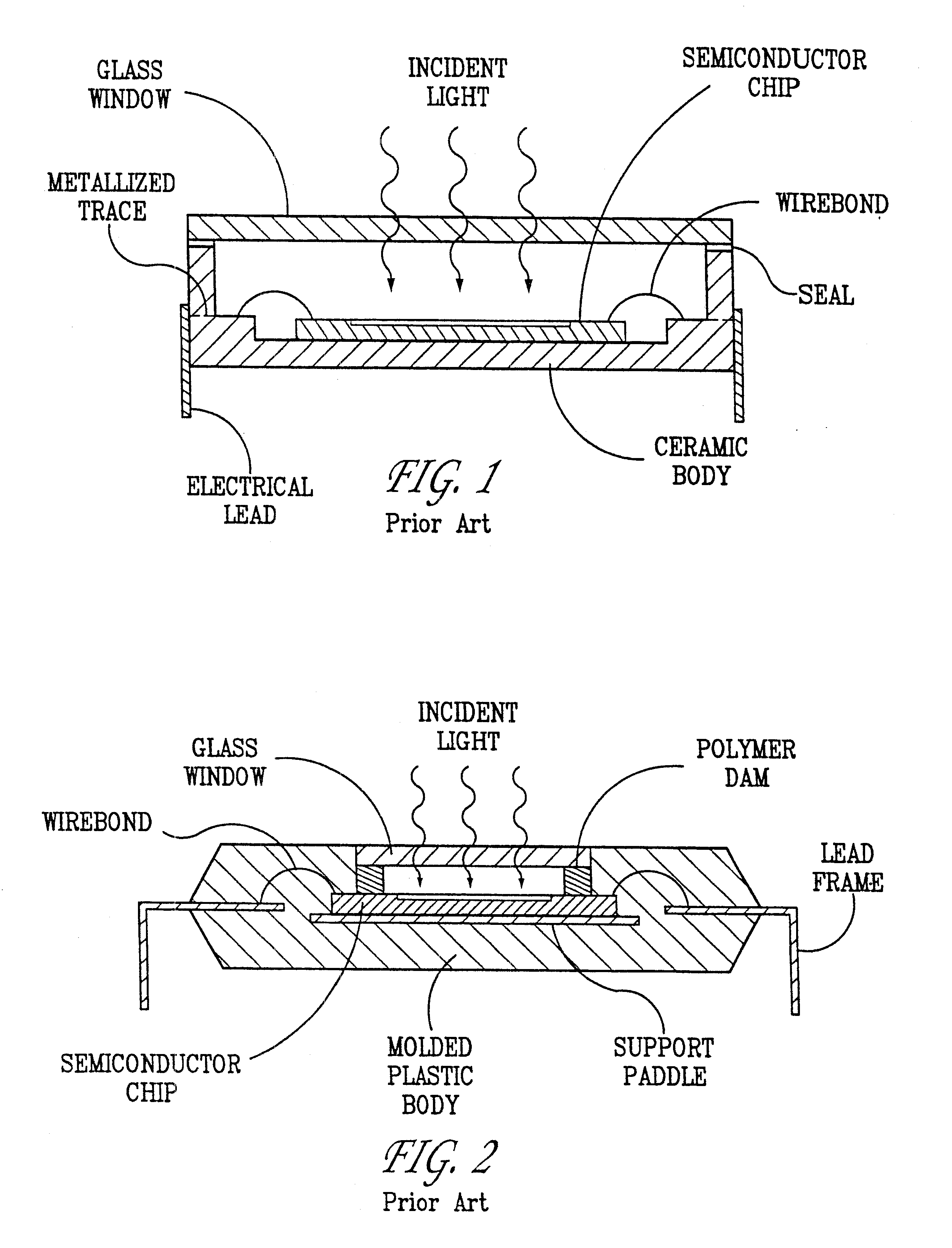
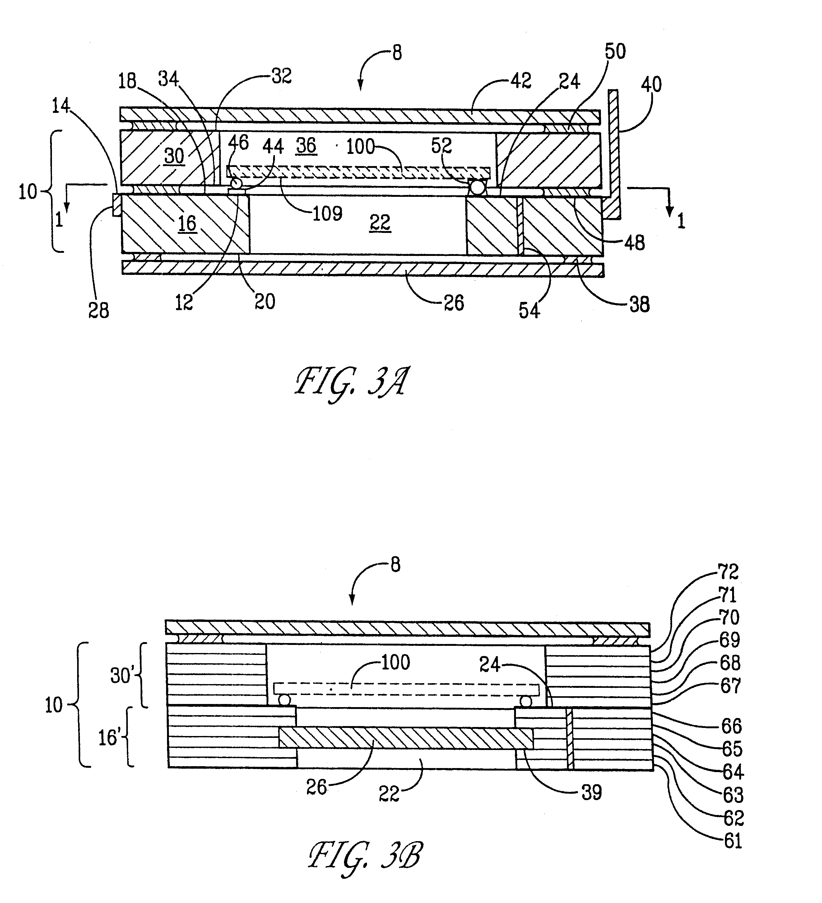
It should be noted that the examples of the present invention shown in the figures are sometimes illustrated with the window facing down, which is the preferred orientation during flip-chip bonding. However, those skilled in the art will understand that the completed package can be oriented for use with the window facing upwards. It should also be noted that all of the figures show only a single microelectronic device, illustrated as a microelectronic device or pair of chips. It is intended that the method and apparatus of the present invention should be understood by those skilled in the art as applying equally to a plurality of chips or devices packaged in a one-dimensional or a two-dimensional array, as in a multi-chip module (MCM), including multiple windowed-compartments, and including having a...


PUM


Abstract

A bi-level, multilayered package with an integral window for housing a microelectronic device. The device can be a semiconductor chip, a CCD chip, a CMOS chip, a VCSEL chip, a laser diode, a MEMS device, or a IMEMS device. The multilayered package can be formed of a low-temperature cofired ceramic (LTCC) or high-temperature cofired ceramic (HTCC) multilayer processes with the window being simultaneously joined (e.g. cofired) to the package body during LTCC or HTCC processing. The microelectronic device can be flip-chip bonded and oriented so that the light-sensitive side is optically accessible through the window. A second chip can be bonded to the backside of the first chip, with the second chip being wirebonded to the second level of the bi-level package. The result is a compact, low-profile package, having an integral window that can be hermetically-sealed.

Description

BACKGROUND OF THE INVENTIONThe present invention relates generally to the field of microelectronics, and more specifically to packaging of microelectronic devices in a package having an integral window.Many different types of microelectronic devices require a window to provide optical access and protection from the environment. Examples of optically-interactive semiconductor devices include charge-coupled devices (CCD), photo-sensitive cells (photocells), solid-state imaging devices, and UV-light sensitive Erasable Programmable Read-Only Memory (EPROM) chips. All of these devices use microelectronic devices that are sensitive to light over a range of wavelengths, including ultraviolet, infrared, and visible. Other types of semiconductor photonic devices emit light, such as laser diodes and Vertical Cavity Surface-Emitting Laser (VCSELS), which also need to pass light through a protective window.Microelectromechanical systems (MEMS) and Integrated MEMS (IMEMS) devices (e.g. MEMS devi...

Claims


Application Information

Patent Timeline
IPC IPC(8): B81B7/00H01L23/053H01L23/10H01L23/02H01L25/10H05K1/18H05K1/02
CPCB81B7/0067H01L23/053H01L23/10H01L25/105H01L27/14618H01L27/14636H01L2224/16H01L2224/48091H01L2224/48227H01L2224/48247H01L2224/49109H01L2924/01004H01L2924/01012H01L2924/0102H01L2924/01025H01L2924/01029H01L2924/01046H01L2924/01077H01L2924/01078H01L2924/01079H01L2924/04941H01L2924/09701H01L2924/15153H01L2924/15165H01L2924/15787H01L2924/16195H01L2924/16235H01L2924/16788H01L2924/19041H01L2924/30107H05K1/02H05K1/181H01L2924/00014H01L2924/00H01L24/48H01L24/49H01L2924/01019H01L2924/01322H01L2225/1058H01L2924/12041H01L2224/16225H01L2924/10253H01L2224/32145H01L2224/73265H01L2924/00015H01L2924/181H01L2924/14H01L2924/1627H01L2224/05599H01L2224/85399H01L2224/45099H01L2924/00012H01L2224/0401H01L2224/45015H01L2924/207
Inventor PETERSON, KENNETH A.WATSON, ROBERT D.
Owner NAT TECH & ENG SOLUTIONS OF SANDIA LLC
Why Eureka
Try Eureka