Integrated circuit carrier arrangement for reducing non-uniformity in current flow through power pins

a technology of integrated circuit and power pins, which is applied in the association of printed circuit non-printed electric components, electrical apparatus construction details, instruments, etc., can solve the problems of increasing power consumption of many integrated circuit devices, requiring packages with hundreds of pins, and consuming tens of watts of power

Inactive Publication Date: 2002-12-17
GLOBALFOUNDRIES INC
View PDF12 Cites 13 Cited by
  • Summary
  • Abstract
  • Description
  • Claims
  • Application Information

AI Technical Summary

Problems solved by technology

The power consumption of many integrated circuit devices has increased as a result of ever higher levels of integration, and ever increasing speeds achievable.
As a result, devices are commonly available having power dissipations that previously would have been unprecedented.
For example, high performance processor devices today dissipate tens of watts and require packages having hundreds of pins.
While such maximum current flow limits may be problematic for many kinds of integrated circuits, the problems are particularly worrisome in the case of modern CPU devices, where the amount of current consumed is typically so much greater than with other kinds of devices.
Previously, the current limitations per power pin were rarely exceeded, even when scant attention was paid to the amount of current flowing through each power pin.
However, ceramic PGA packages have significantly higher power plane resistance (e.g., 10 milliOhm per square) which significantly affects the pattern of current flow in the package power planes.
Similarly, the use of multiple power planes in parallel also achieves a lower effective resistance.
But such options are not always available when designing packages.
In spite of the long history of package designs that accommodate high pin-count and relatively high-current devices, the particular problems of high current flow through package and / or connector power pins become more difficult with each new generation of microprocessors.
Even though an integrated circuit package has a large number of power pins allocated to an internal power plane, the current flowing through the power pins may divide very unevenly, and result in current flow through some of the power pins which exceeds the maximum specification for either the package pin or for the socket into which the package may be inserted.

Method used


Image

  • Integrated circuit carrier arrangement for reducing non-uniformity in current flow through power pins
  • Integrated circuit carrier arrangement for reducing non-uniformity in current flow through power pins
  • Integrated circuit carrier arrangement for reducing non-uniformity in current flow through power pins

Examples


Embodiment Construction

)

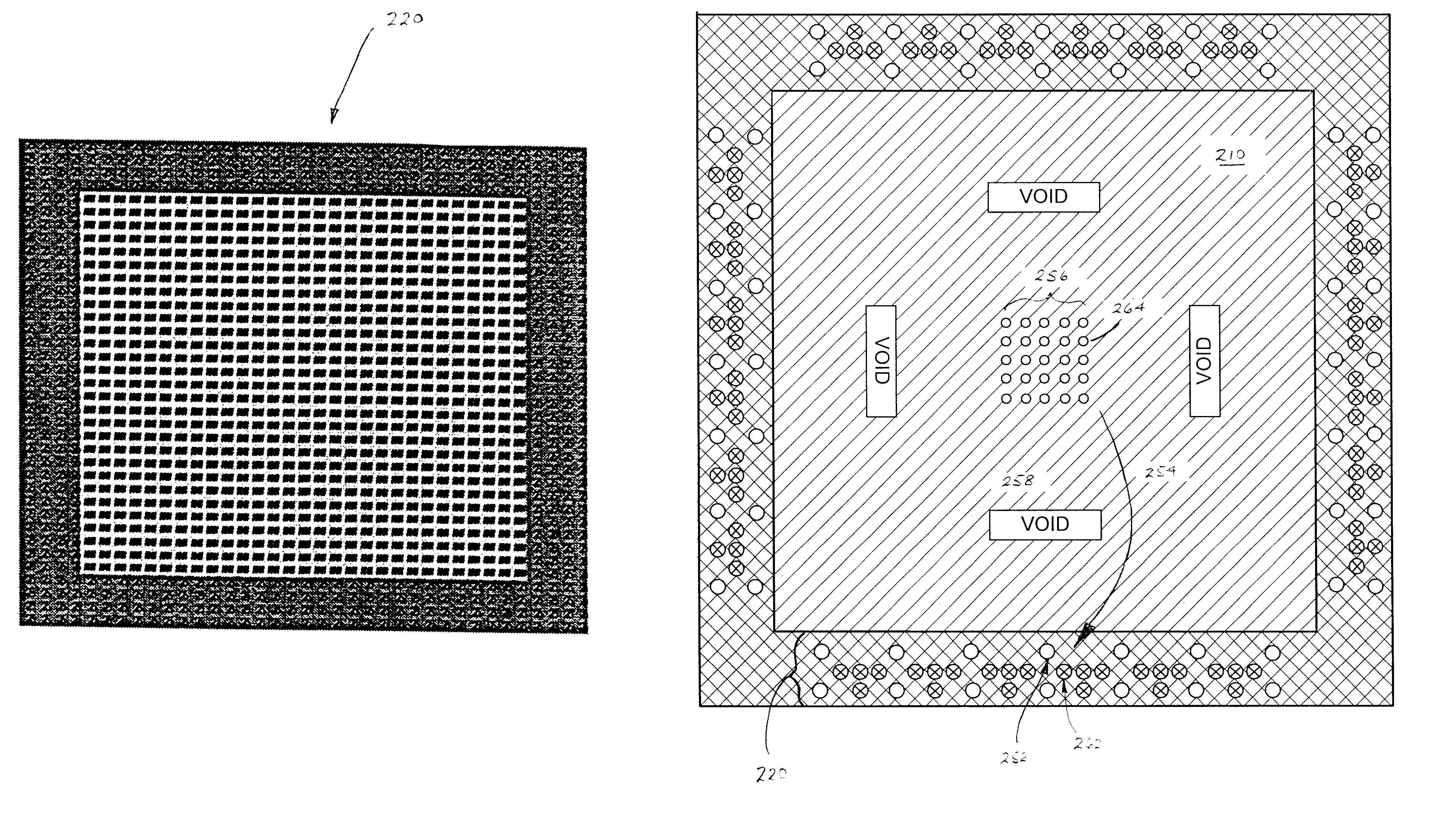
An analysis method was devised to model an integrated circuit die assembled in a PGA package which is inserted into a socket on a motherboard. The method may be used to calculate the current through each power pin of a PGA package (and the corresponding socket pin) as a function of: (1) the location of each power pin within the package; (2) the location of the power terminal connection(s) on the motherboard which provides the power to the motherboard power plane; (3) the resistivity of the power planes in both the motherboard and in the package; and (4) the extent and shape of each such power plane, especially the power plane within the package.

A mathematical spreadsheet model was devised to solve for the current distribution within the power planes and through each of the power pins. In the model, each power plane is divided into elements, such as a 1.27.times.1.27 mm square region (50 mils.times.50 mils). This grid size facilitates modeling a common package pin center-to-center s...


PUM


Abstract

In an integrated circuit carrier having a large number of power pins allocated to an internal power plane, the current flowing through the power pins may divide very unevenly, and result in current flow through some of the power pins which exceeds the maximum specification for either the package pin or for the socket into which the package may be inserted. In such a package, the magnitude of the current flowing through the highest current power pin may be reduced by configuring the resistance of the power plane(s) and vias to provide approximately the same total resistance to every power pin location. Slots may be cut in a package power plane to alter the current path and raise the impedance of the conduction path between some of the package power pins and the internal contact pads otherwise having the lowest impedance. If the package, such as a pin-grid-array package, includes more than one row of pins along an edge of the package, the internal package vias may be arranged to provide an impedance from die footprint to the outer row of pins which is not substantially higher than that of the inner row of pins. In this fashion the aggregate current carrying capacity of the carrier may be increased by reducing the difference in current flow between power pins having the highest current flow and power pins having the lowest current flow. The current flow through all the power pins may then be operated nearer to the design maximum of the particular connector used, or the design maximum of the carrier itself.

Description

1. Field of the InventionThe present invention relates to conductive planes within an integrated circuit carrier, such as a pin grid array package, for conveying power / ground to an integrated circuit attached to the carrier, and particularly relates to improving uniformity in current flowing through each of a plurality of external electrodes of the carrier connected to such a conductive plane.2. Description of the Related ArtIntegrated circuit carriers are well known in the art, and a wide variety of such integrated circuit carriers are readily available. Each type of carrier provides a physical body to which an integrated circuit die is attached, and usually affords a moderate to great deal of physical protection for the integrated circuit die. Frequently such integrated circuit carriers provide an enclosure having a cavity within which the die is attached and which is then covered by a protective lid. Other integrated circuit carriers protect an attached die using a molded plastic...

Claims


Application Information

Patent Timeline
Patent Type & Authority Patents(United States)
IPC IPC(8): H01L23/48H01L23/50
CPCH01L23/50H01L2924/3011H01L2924/0002H01L2924/00
Inventor HERRELL, DENNIS J.HIRSCH, THOMAS J.
Owner GLOBALFOUNDRIES INC
Why Eureka
Try Eureka