Arrangement relating to electronic circuitry

a technology of electronic circuits and arrangement, applied in the direction of high frequency circuit adaptation, waveguide type devices, cross-talk/noise/interference reduction, etc., can solve the problems of reducing the bandwidth of the circuit, limiting the rf performance, and e.g. bandwidth,

Inactive Publication Date: 2002-12-31
TELEFON AB LM ERICSSON (PUBL)
View PDF7 Cites 26 Cited by
  • Summary
  • Abstract
  • Description
  • Claims
  • Application Information

AI Technical Summary

Benefits of technology

Yet another object of the present invention is to achieve a method for producing a multilayered RF-circuit with improved yield.
This results in a less expensive circuit, since its fault tolerant qualities provide higher yield in a given manufacturing process.
It also allows multilayered RF-circuits with improved bandwidth properties to be produced at a relatively low cost.
This results in a manufacturing process producing multilayered RF-circuits with improved yield.

Problems solved by technology

A problem with this kind of transition is that the capacitance per length unit between the signal conductor and the ground conductor often is lower in the transition region as compared to the horizontally extending transmission line parts.
This results in reflections when a signal having a predetermined frequency is propagated in the transmission line towards the transition region.
The transition, thus, is not matched and this limits the RF performance, e.g. bandwidth, of the circuit.
This causes a problem with the above-described compensation arrangement.
A relatively small displacement, positioning a segment part of the via conductor a bit closer to the planar ground conductor may render the compensating capacitance far too large.
This is likely to reduce the bandwidth of the circuit to such an extent that it is useless for the intended purposes.
A transition designed to be fully compensated in the ideal position will therefore have a relatively low yield when produced, i.e. only a relatively small number of circuits in a batch of a given size will function properly.
This, of course, makes the circuits very expensive.
This results in higher yield but smaller bandwidth.
Thus, a trade-off between yield and RF performance, e.g. bandwidth, exists

Method used


Image

  • Arrangement relating to electronic circuitry
  • Arrangement relating to electronic circuitry
  • Arrangement relating to electronic circuitry

Examples


Embodiment Construction

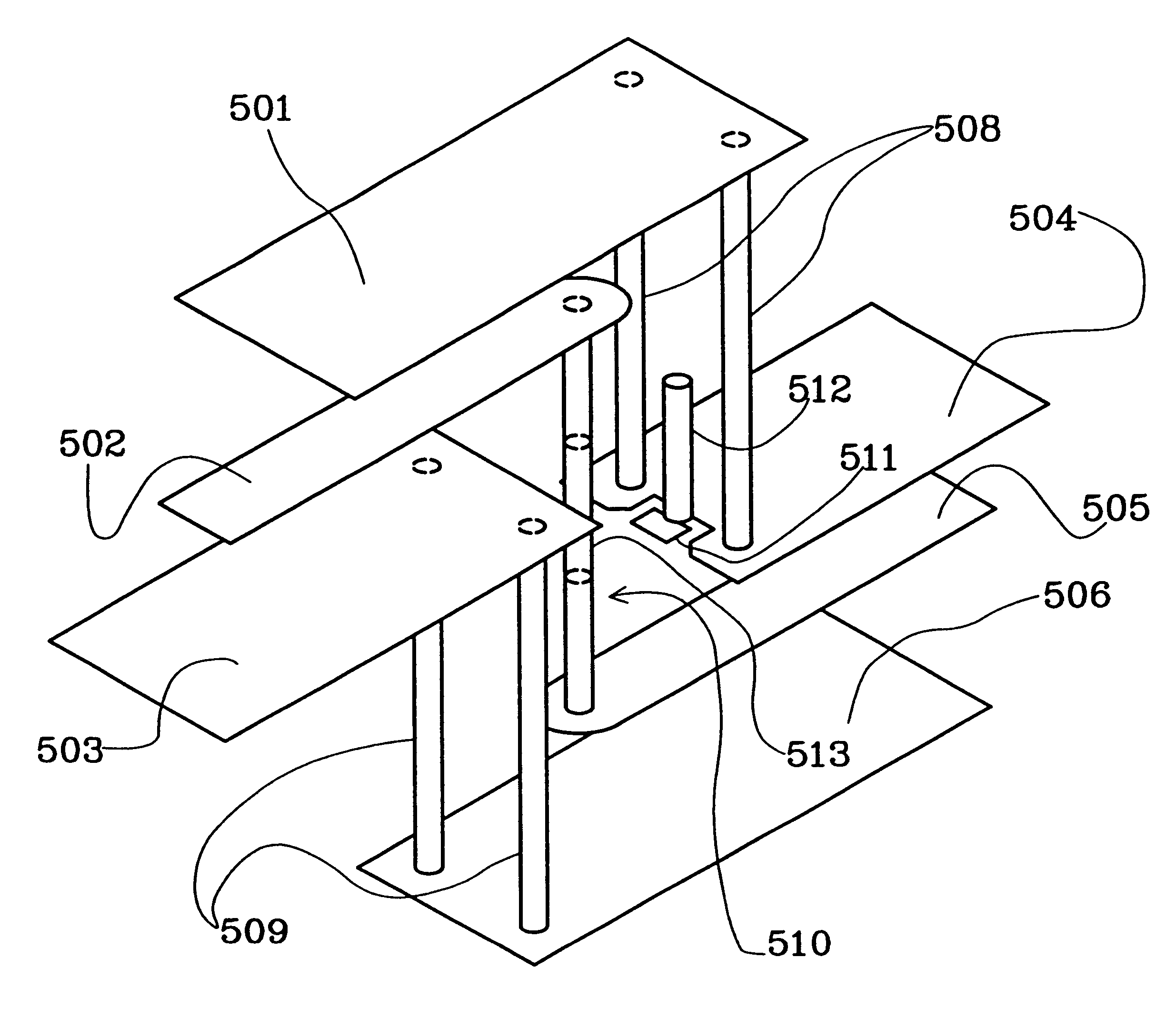
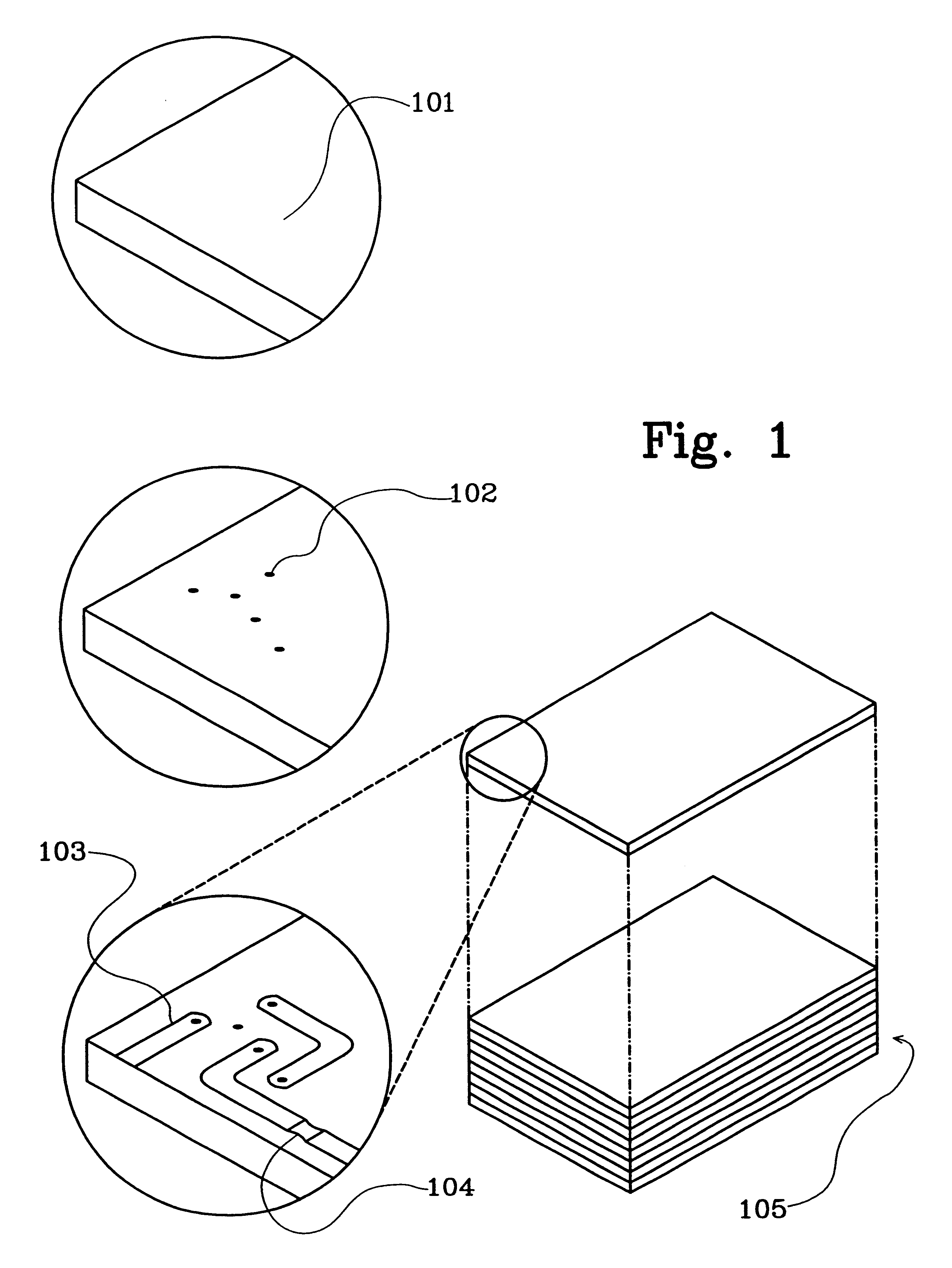
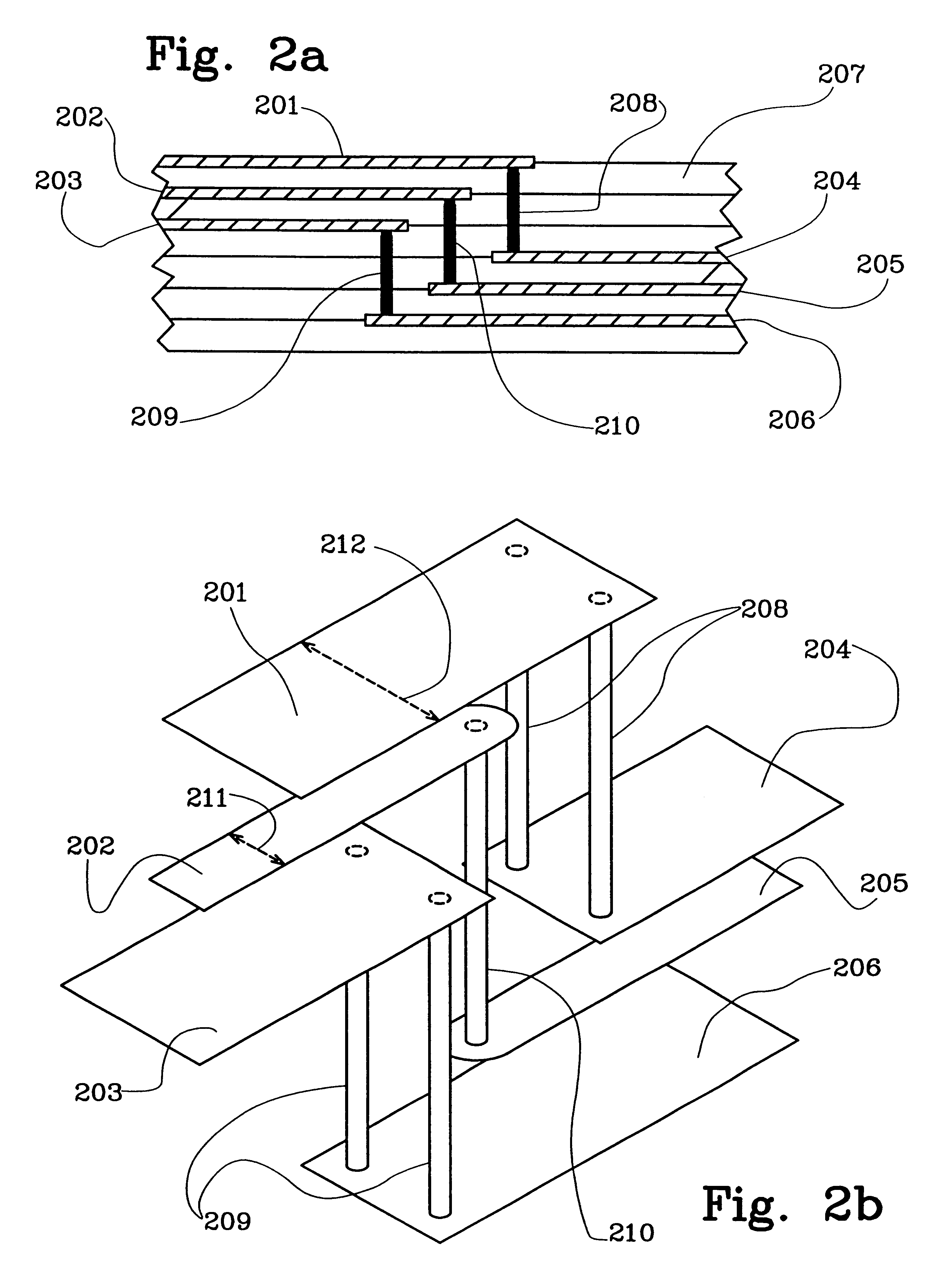
FIG. 1 illustrates some steps in an LTCC process. The substrate sheets 101 used in the process are preferably made of a thin dielectric ceramic material. In a first step, holes 102 are punched in predetermined patterns in these substrates 101. These holes 102 are filled with a suitable conductive material, such as for instance gold. Then conductors 103 are printed on one or in some cases two sides of the substrate by using a screen printing process. Components 104 such as resistors may also be disposed on the substrate 101. In circuits operating at microwave frequencies, components such as capacitances and filters of different kinds may often be formed by different configurations of planar conductors.

When all substrate sheets are prepared they are stacked into a pile 105. The pile 105 may include up to more than 40 layers, but 10 is considered a more normal number. The pile 105 may be laminated and preheated before it is fired in an oven at around 850.degree. C., typically for about...


PUM


Abstract

The present invention relates to an arrangement in a multilayered electronic circuit. In a transition between two planar transmission lines, a compensating element is used to keep the average capacitance per length unit more constant during the transition. A via conductor the passes near an edge of a planar conductor pattern, the via conductor and the planar conductor having a mutual capacitive coupling within a predetermined range. A compensating conductor is formed between the planar conductor and the via conductor, which conductor is connected to the planar conductor by a compensating via. If the segment of the via conductor which belongs to the same via hole pattern as the compensating via is displaced, the compensating via is also displaced. The compensating planar pattern is then disconnected from the planar conductor. This improves yield in a given multilayer process.

Description

This application claims priority under 35 U.S.C. .sctn..sctn.119 and / or 365 to 9904527-0 filed in Sweden on Dec. 10, 1999; the entire content of which is hereby incorporated by reference.The present invention relates to an arrangement in a multilayered electronic circuit for radio frequency applications, as well as a method of manufacturing such a circuit and a RF-circuit comprising such an arrangement.DESCRIPTION OF RELATED ARTMultilayered RF-circuits are used more and more in communications technology and elsewhere. The reason for this is that they allow smaller circuits to be built. One process resulting in multilayered RF-circuits is the LTCC process, an abbreviation for Low Temperature Cofired Ceramics. This process generally involves steps as follows. First holes are punched in predetermined patterns in a number of substrates. The holes are filled with a conductive material. When the circuit is finished, this material forms vias, which provide for vertical transitions within t...

Claims


Application Information

Patent Timeline
Patent Type & Authority Patents(United States)
IPC IPC(8): H01L23/58H01L23/64H01L23/522H01L23/52H01L23/66H01P1/04H05K1/02
CPCH01L23/5222H01L23/642H01L23/66H01P1/047H05K1/0251H01L2223/6616H01L2924/09701H05K1/0219H05K2201/093H05K2201/09618H05K2201/09781H05K2201/09809H05K2201/09845H01L2924/0002H01L2924/00
Inventor ALBINSSON, BJORN
Owner TELEFON AB LM ERICSSON (PUBL)
Why Eureka
Try Eureka