Micro-optoelectromechanical system based device with aligned structures and method for fabricating same

a micro-optoelectromechanical and system-based technology, applied in the direction of optical waveguide light guide, instruments, optics, etc., can solve the problems of difficult alignment of structures fabricated in different structural layers, difficult to achieve alignment accuracy needed for high-efficiency coupling with micro-optoelectromechanical system-based devices

Inactive Publication Date: 2003-01-21
XEROX CORP
View PDF5 Cites 16 Cited by
  • Summary
  • Abstract
  • Description
  • Claims
  • Application Information

AI Technical Summary

Problems solved by technology

Coupling of light signals between an, optical fiber and an optical system has been a challenging issue in the design of optical systems for optical fiber communication.
It is difficult to achieve alignment of structures fabricated in different structural layers with an accuracy better than 1 micron.
Thus, it is difficult to the alignment accuracy needed for high efficiency coupling with micro-optoelectromechanical system-based devices.
Such adjustment is labor intensive and costly.

Method used


Image

  • Micro-optoelectromechanical system based device with aligned structures and method for fabricating same
  • Micro-optoelectromechanical system based device with aligned structures and method for fabricating same
  • Micro-optoelectromechanical system based device with aligned structures and method for fabricating same

Examples


Embodiment Construction

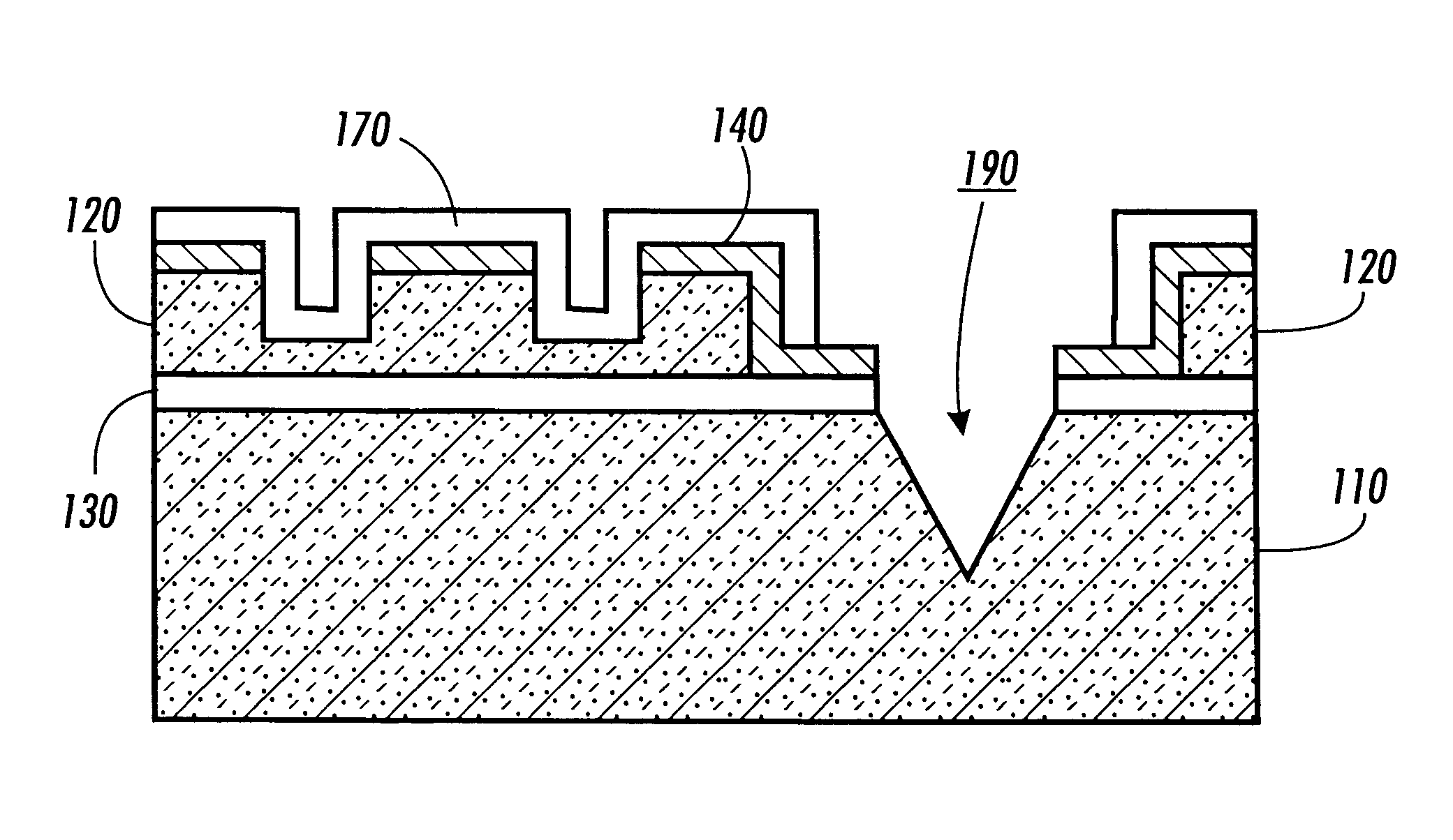
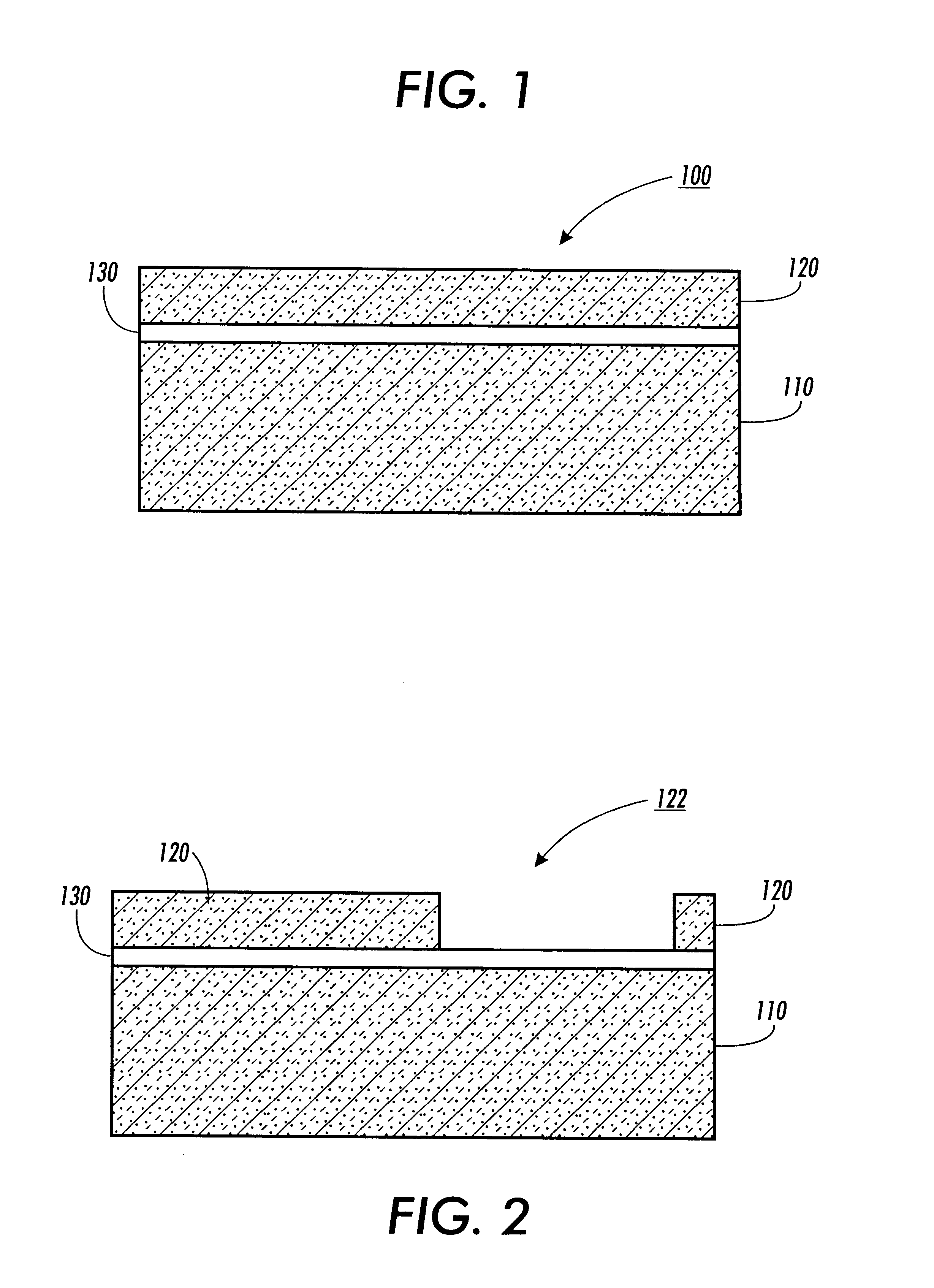
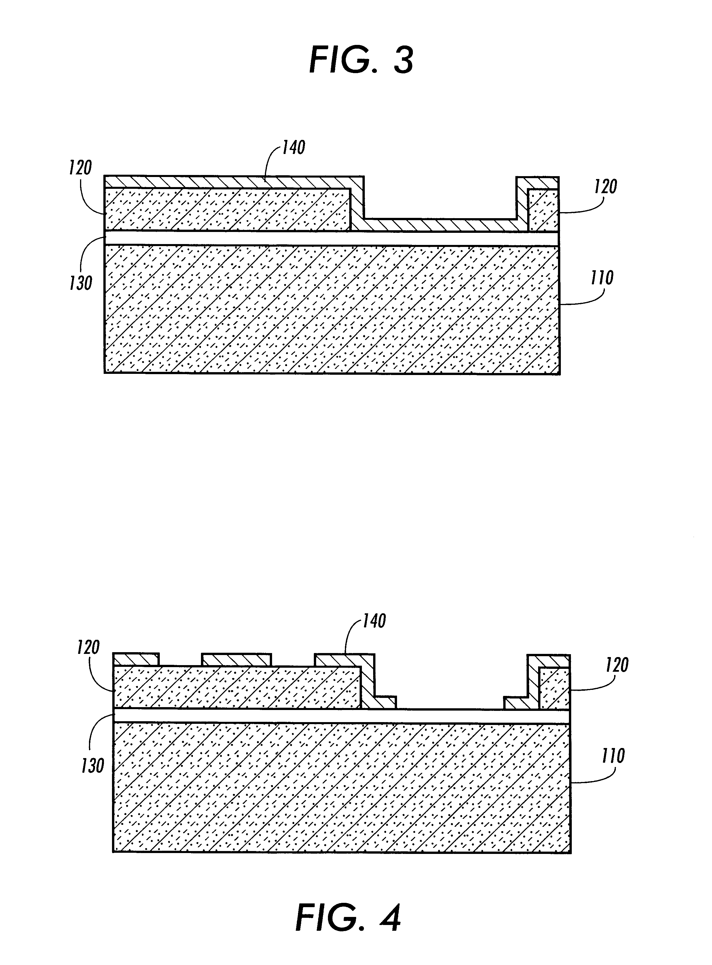
This invention provides micro-optoelectromechanical system based devices with aligned structures. According to the invention, the device comprises at least one optical structure formed in a silicon layer of the device and at least one optical fiber connection structure that is self-aligned with the at least one optical structure. In various exemplary embodiments, the at least one optical fiber connection structure is formed in a substrate of the device. The at least one optical fiber connection structure may comprise a V-groove. In other embodiments, the at least one optical structure may comprise a waveguide. A nitride layer may be formed on at least a portion of the waveguide. In various embodiments, the silicon layer may be a single-crystal-silicon layer of a silicon-on-insulator wafer.

This invention also provides methods for fabricating a micro-optoelectromechanical system based device with aligned structures. According to the invention, at least one optical structure is defined...


PUM


Abstract

A micro-optoelectromechanical system based device with aligned structures comprises at least one optical structure formed in a silicon layer of the device and at least one optical fiber connection structure that is self-aligned with the at least one optical structure. In embodiments, the at least one optical fiber connection structure is formed in a substrate of the device and may comprise a V-groove. In other embodiments, the at least one optical structure may comprise a waveguide. A nitride layer may be formed on at least a portion of the waveguide. In various embodiments, the silicon layer may be a single-crystal-silicon layer of a silicon-on-insulator wafer. A method for fabricating a micro-optoelectromechanical system based device with aligned structures is provided in which the at least one optical structure and the at least one optical fiber connection structure are defined using the same masking layer.

Description

1. Field of InventionThis invention relates to optical micromachined or microelectromechanical system based devices with aligned structures and methods for fabricating these structures.2. Description of Related ArtCoupling of light signals between an, optical fiber and an optical system has been a challenging issue in the design of optical systems for optical fiber communication. Strict alignment between optical fibers and optical devices, such as lenses, waveguides, photo-detectors, and the like, is needed to achieve a high coupling efficiency. For example, for single-mode fibers, alignment tolerance is normally less than 1 micron.In particular in a micro-optoelectromechanical system (MOEMS), accurate alignment between various structures is critical to prevent undesirable optical losses. Micro-electromechanical system (MEMS) structures are normally defined on a subsrate with non-planar topography, that is, with various structures defined in different structural layers. It is diffic...

Claims


Application Information

Patent Timeline
Patent Type & Authority Patents(United States)
IPC IPC(8): G02B6/13G02B6/36G02B6/136G02B6/30G02B6/12
CPCG02B6/136G02B6/30G02B6/3692G02B6/3636G02B2006/12097G02B6/3652
Inventor TRAN, ALEXKUBBY, JOEL A.CHEN, JINGKUANGGULVIN, PETERFEINBERG, KATHLEEN A.SU, YI
Owner XEROX CORP
Why Eureka
Try Eureka