Thin film transistor
- Summary
- Abstract
- Description
- Claims
- Application Information
AI Technical Summary
Problems solved by technology
Method used
Image

Examples
Embodiment Construction
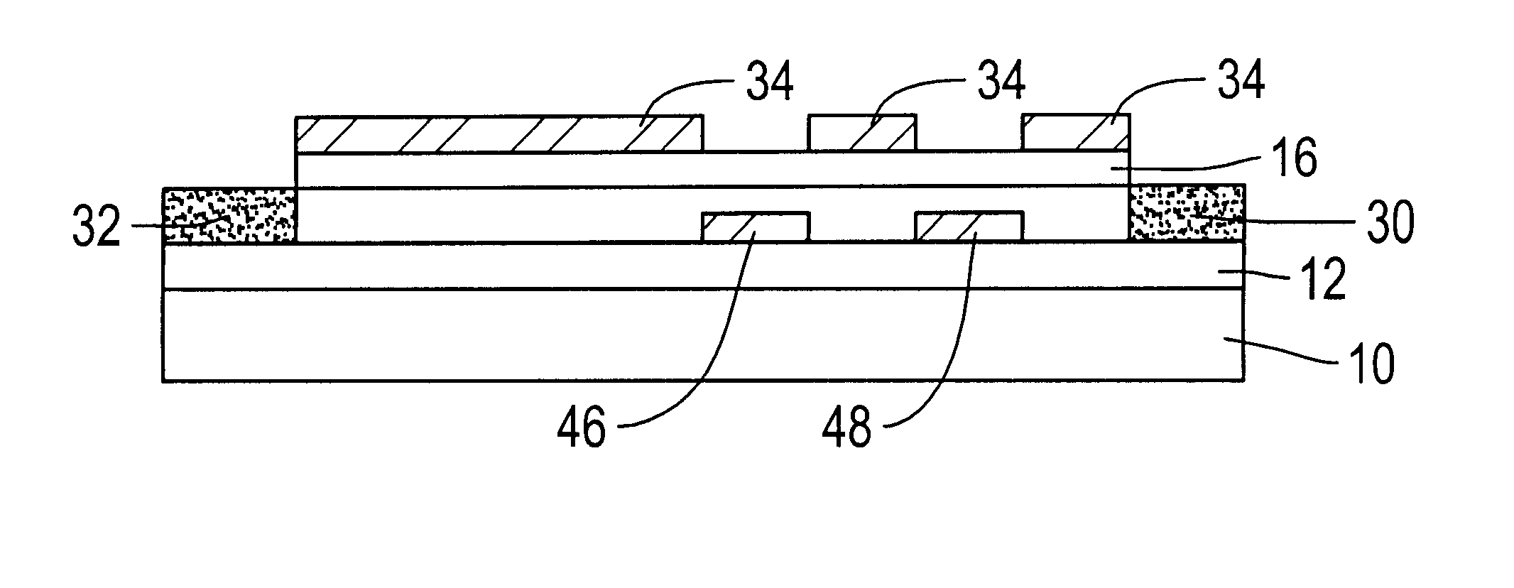
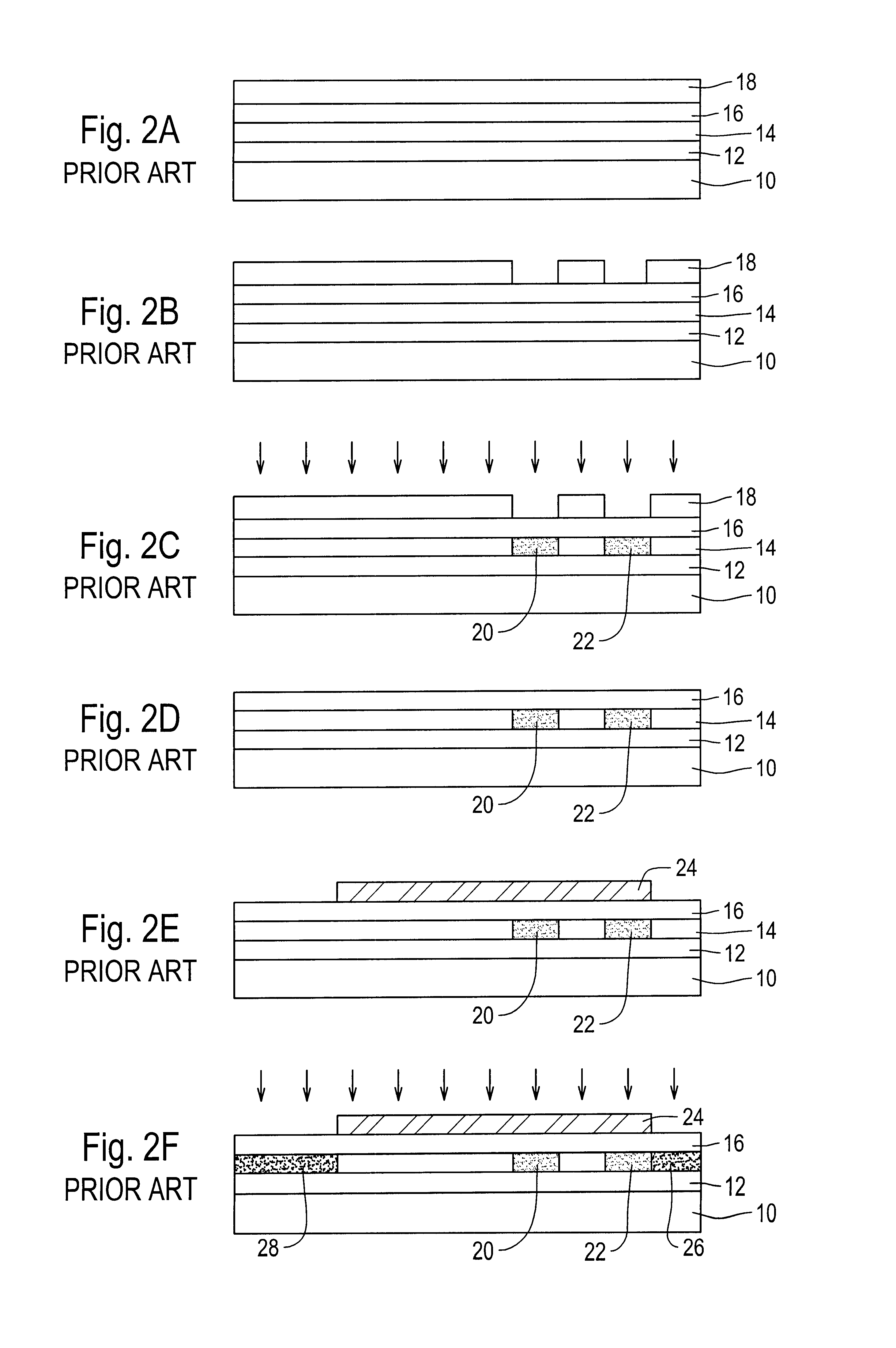
The formation of a gate overlapped lightly doped drain transistor will now be described with reference to FIG. 2. First, as shown in FIG. 2(a), a basic layered arrangement of: a substrate 10, a buffer oxide layer 12, an active layer of silicon 14, a gate oxide layer 16, and a mask 18 are built up in that order using known techniques. The mask layer 18 is then patterned as shown in FIG. 2(b). That is, two openings are formed in the mask such that ion implantation can be effected to form two lightly doped regions, 20 and 22, in the active layer 14; as shown in FIG. 2(c). Next the mask layer 18 is removed, as shown in FIG. 2(d). A metal is then deposited and patterned so as to form the gate electrode 24, as shown in FIG. 2(e). As shown in FIG. 2(e), the rightmost end of the gate electrode 24 is approximately aligned with the rightmost end of the lightly doped region 22. A further stage of implantation is then performed, as shown in FIG. 2(f), so as to form the heavily doped drain 26 an...
PUM
 Abstract
Description
Claims
Application Information
 - R&D Engineer
- R&D Manager
- IP Professional
- Industry Leading Data Capabilities
- Powerful AI technology
- Patent DNA Extraction
Browse by: Latest US Patents, China's latest patents, Technical Efficacy Thesaurus, Application Domain, Technology Topic.
© 2024 PatSnap. All rights reserved.Legal|Privacy policy|Modern Slavery Act Transparency Statement|Sitemap