Method of fusion for heteroepitaxial layers and overgrowth thereon

a heteroepitaxial layer and fusion technology, applied in the direction of basic electric elements, semiconductor/solid-state device manufacturing, electric devices, etc., can solve the problems of significant deterioration of crystal and optical properties of so-formed substrates, almost impossible to form high-quality crystal layers, and almost impossible to grow gaas having different lattice constants on si substrates or inp substrates without any defects

Inactive Publication Date: 2003-03-18
KOREA INST OF SCI & TECH
View PDF7 Cites 7 Cited by
  • Summary
  • Abstract
  • Description
  • Claims
  • Application Information

AI Technical Summary

Benefits of technology

The object of the present invention is to provide, without significant defects, methods capable of accomplishing good quality epitaxial growth after the junction of two semiconductor materials having different lattice constants.

Problems solved by technology

Generally, it is almost impossible to form a high quality crystal layer with materials having different lattice constants.
Forming a thin film on a substrate by using another material having a lattice constant different from that of the substrate causes defects such as threading dislocation inside the thin film, thereby resulting in significant deterioration of crystal and optical properties of the so-formed substrate.
For example, it is almost impossible for GaAs having different lattice constants to be grown on a Si substrate or an InP substrate without any defects.
However, it is difficult for the interface between two substrates to be free of defects due to the effects of the two substrates.
As a result, a good quality hetero-junction cannot be achieved.
However, a hetero-junction of two semiconductor materials with different lattice constants has the problems mentioned above, and nothing has been published on quantum structure-related technology for heteroepitaxy.

Method used


Image

  • Method of fusion for heteroepitaxial layers and overgrowth thereon
  • Method of fusion for heteroepitaxial layers and overgrowth thereon
  • Method of fusion for heteroepitaxial layers and overgrowth thereon

Examples


Embodiment Construction

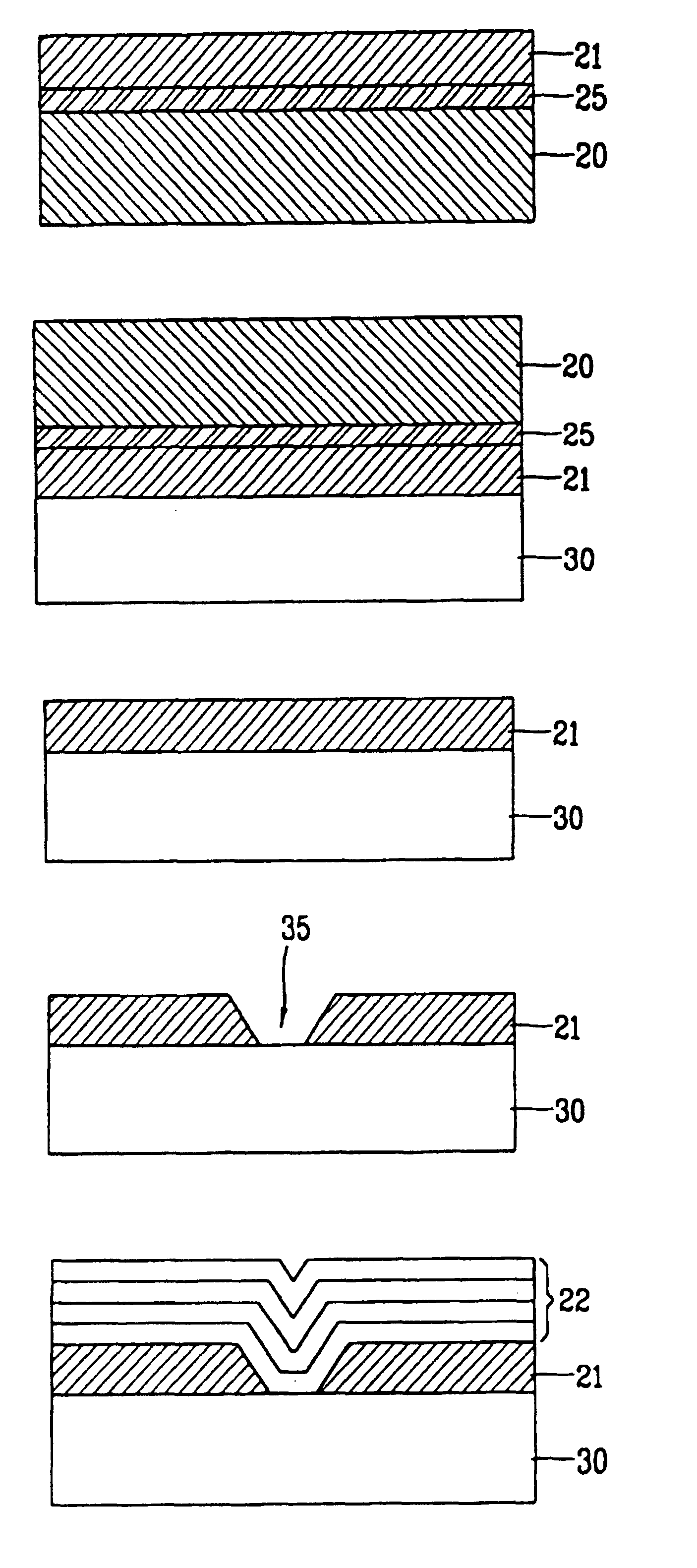
To achieve the above objects, the present invention provides the methods of fusion for heteroepitaxial layers and overgrowth thereon comprising the steps of:

a) forming an epitaxial layer, having a lattice constant similar to that of the first semiconductor substrate, as a sacrificial layer on said first semiconductor substrate;

b) forming an epitaxial layer, consisting of the same material as that of the first semiconductor substrate, as a fusion layer on said sacrificial layer;

c) fusing the fusion layer to a second semiconductor substrate consisting of a material having a lattice constant different from said first semiconductor substrate;

d) separating the first semiconductor substrate from the second semiconductor substrate by removing the sacrificial layer;

e) patterning a U or V shape in the fusion layer; and

f) overgrowing multi-layers consisting of materials with a lattice constant that is the same as or similar to that of the fusion layer on the patterned fusion layer.

The first s...


PUM

PropertyMeasurementUnit
widthaaaaaaaaaa
pressureaaaaaaaaaa
temperatureaaaaaaaaaa

Abstract

The present invention relates to a method of fusion for heteroepitaxial layers and overgrowth thereon. According to the present invention, a high quality heteroepilayer can be formed by patterning a fused semiconductor layer, overgrowing it with a persistent patterned character, and fusing other semiconductors having different lattice constants by means of utilizing the rate difference between the lateral growth rate and the vertical growth rate exhibited, on the above process. Further, according to the present invention, the lattice constant difference of the two semiconductors can be overcome and a high quality quantum structure can be formed. According to the present invention, the junction of two semiconductor materials having different lattice constants, as well as a good overgrowth on heteroepitaxial layers can be carried out. Accordingly to the present invention, the base material from which the new, as yet on realized, conceptive optoelectronic device can be made.

Description

1. Field of the InventionThe present invention relates to methods of fusion for heteroepitaxial layers and overgrowth thereon. More particularly, the present invention relates to methods of forming a high quality epitaxial layer on the heteroepitaxy with materials having different lattice constants and heteroepitaxy so fabricated.2. Description of the Prior ArtGenerally, it is almost impossible to form a high quality crystal layer with materials having different lattice constants. Forming a thin film on a substrate by using another material having a lattice constant different from that of the substrate causes defects such as threading dislocation inside the thin film, thereby resulting in significant deterioration of crystal and optical properties of the so-formed substrate. For example, it is almost impossible for GaAs having different lattice constants to be grown on a Si substrate or an InP substrate without any defects. However, if defect-free growth can be realized, high integr...

Claims


Application Information

Patent Timeline
Patent Type & Authority Patents(United States)
IPC IPC(8): H01L21/20H01L21/02H01L21/762H01L21/70
CPCH01L21/02381H01L21/02392H01L21/02463H01L21/02494H01L21/76251H01L21/02658H01L21/2007H01L21/76248H01L21/02546H01L21/20
Inventor PARK, YOUNG-JUHWANG, SUNG-MINKIM, EUN-KYU
Owner KOREA INST OF SCI & TECH
Why Eureka
Try Eureka