Level shifting, scannable latch, and method therefor

a level shifting and latch technology, applied in the field of latch circuitry, can solve the problems of consuming more power, occupying more space, and consuming more power, and achieving the effect of reducing the number of latches

Inactive Publication Date: 2003-04-08
IBM CORP
View PDF4 Cites 46 Cited by
  • Summary
  • Abstract
  • Description
  • Claims
  • Application Information

AI Technical Summary

Problems solved by technology

As systems-on-a-chip become more complex, the circuitry on a chip is increasingly put together from disparate designs.
High-performance designs for such level shifting circuitry are more difficult for the case where an input s...

Method used


Image

  • Level shifting, scannable latch, and method therefor
  • Level shifting, scannable latch, and method therefor
  • Level shifting, scannable latch, and method therefor

Examples


Embodiment Construction

The claims at the end of this application set out novel features which applicants believe are characteristic of the invention. The invention, a preferred mode of use, further objectives and advantages, will best be understood by reference to the following detailed description of an illustrative embodiment read in conjunction with the accompanying drawings.

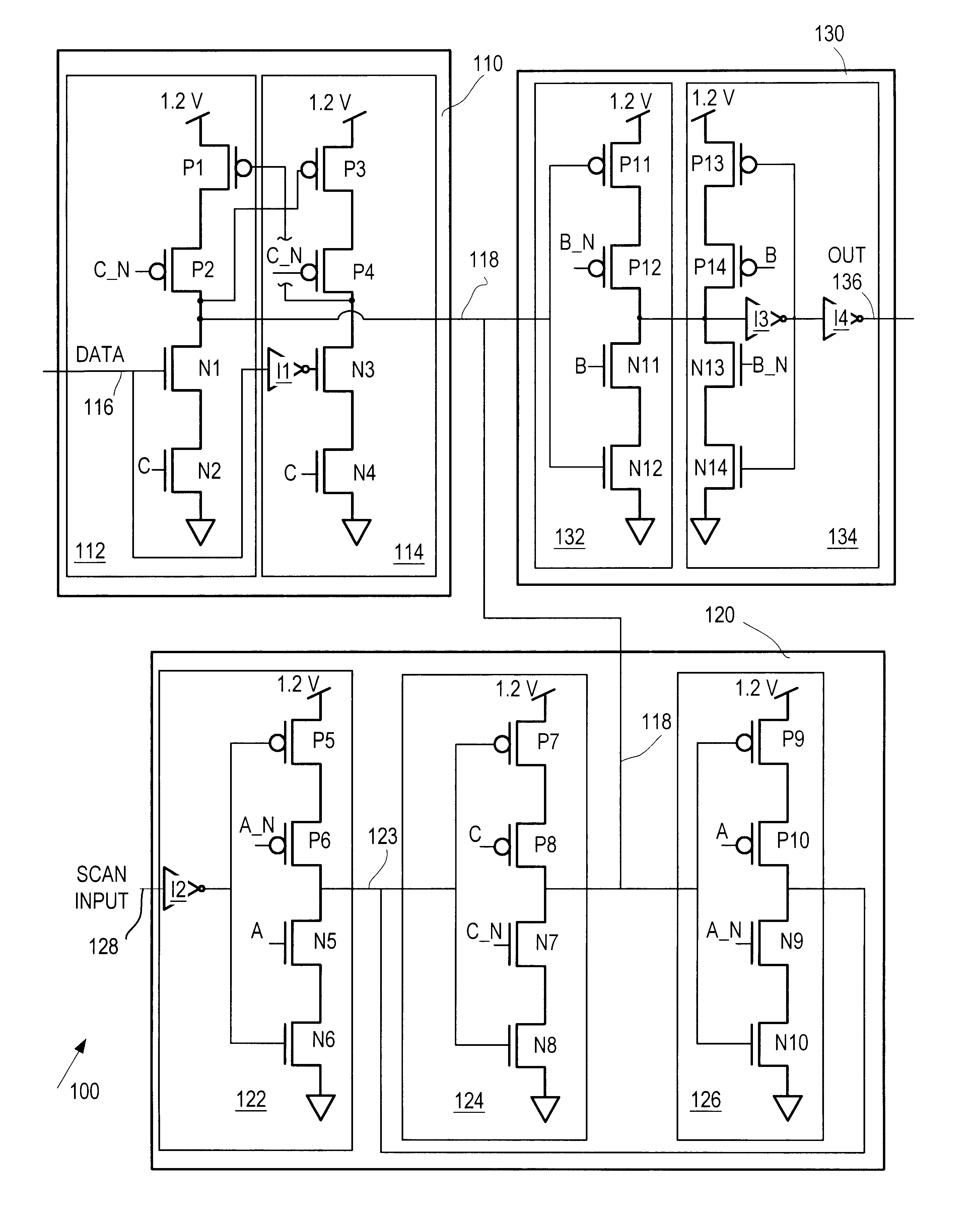
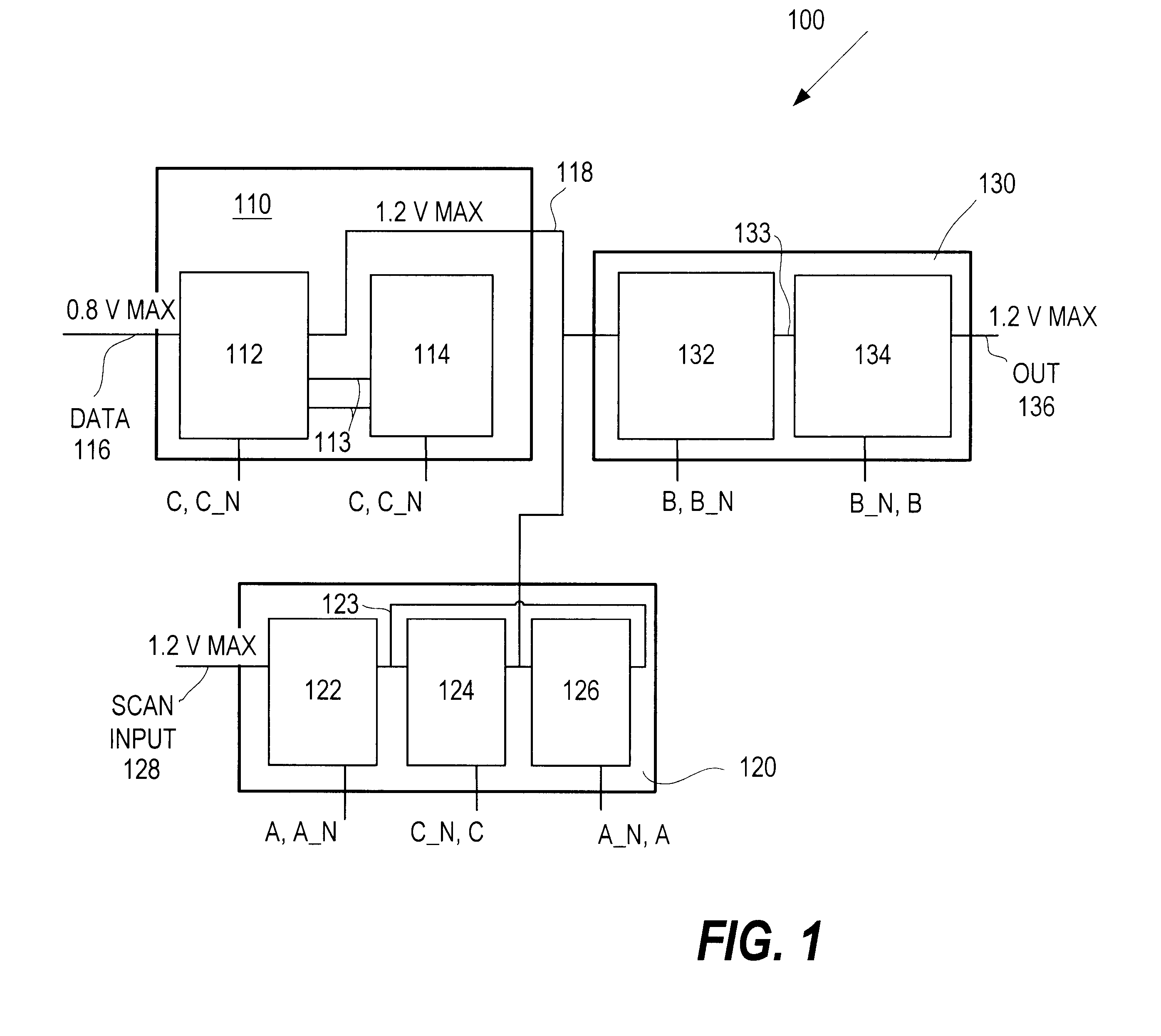
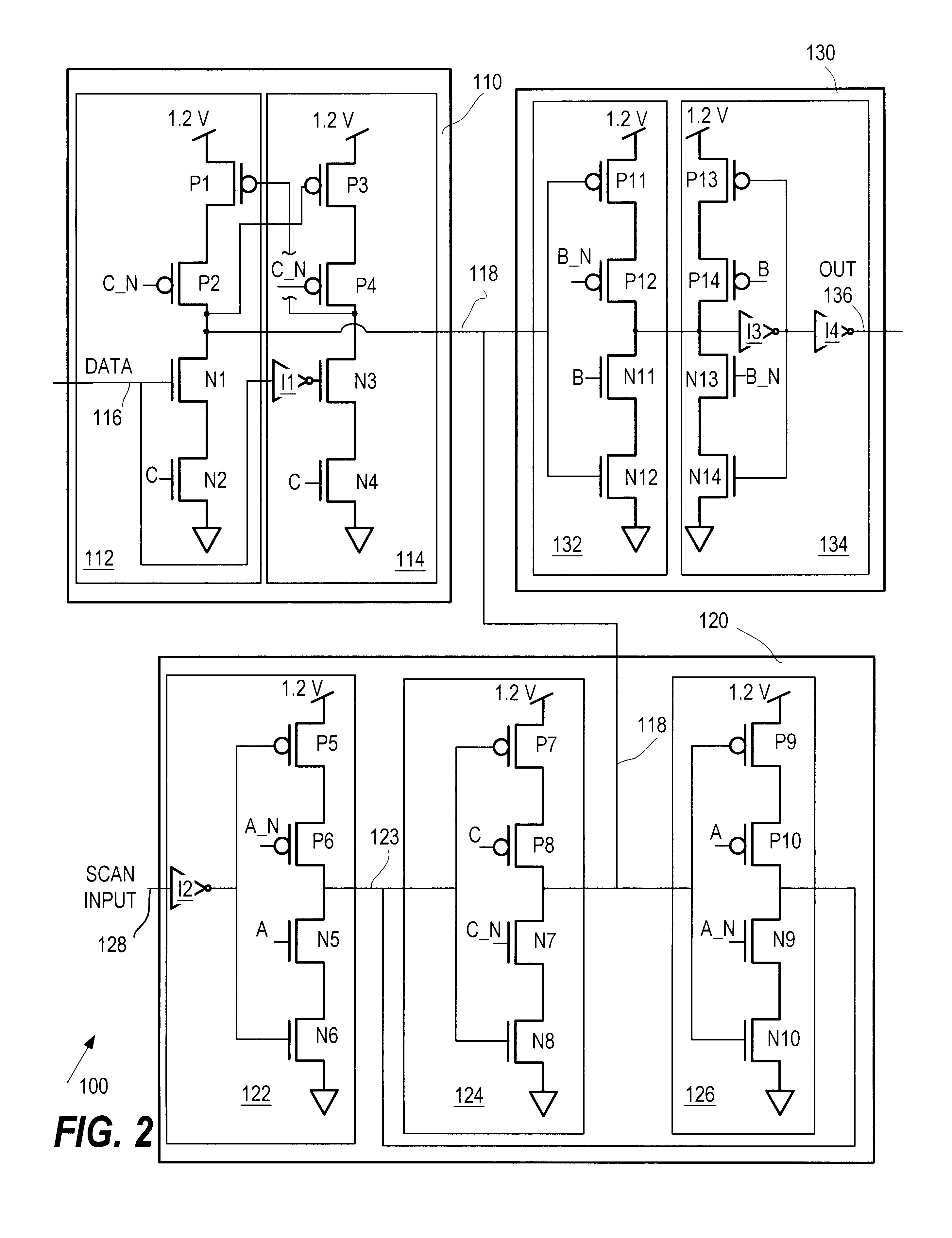
Referring now to FIG. 1, a block diagram of latch circuitry 100 is shown, according to an embodiment of the present invention. "Latch circuitry," as the term is used herein, is circuitry which operates in cycles responsive to at least one timing signal. During a cycle the latch circuitry captures an input signal, that is, "data," at a latch input and holds the data at the latch output.

The latch circuitry 100 has a first input stage 110 for sampling a first input signal on an input node, that is, "data" 116, responsive to a clock signal C and a complement of the clock signal, C_N. The first input stage 110 has a first section 112 an...


PUM


Abstract

Latch circuitry has a data input stage for sampling a first input signal responsive to a first timing signal and generating a signal on an intermediate node in the latch circuitry. The latch circuitry also has a scan input stage for sampling a second input signal responsive to a second timing signal, and generating a signal on the intermediate node. The latch circuitry also has an output stage for generating an output signal on an output node of the latch circuitry responsive to the signal on the intermediate node and a third timing signal. The data input signal has a maximum voltage level and at least one stage of the latch circuitry is operable to effectively shift the voltage level so that the output signal has a higher maximum voltage level than that of the data input signal.

Description

1. Field of the InventionThis invention concerns latch circuitry and more particularly concerns latch circuitry that apertures an input signal, i.e., "data," and outputs a signal having a higher maximum voltage level, in effect shifting the maximum voltage level of the input signal.2. Related ArtAs systems-on-a-chip become more complex, the circuitry on a chip is increasingly put together from disparate designs. Moreover, to reduce power consumption on a chip it is common include some portions of logic circuitry that operate at a lower voltage (and thus lower power), and other portions, such as analog circuits or critical high speed circuits, that operate at a higher voltage due to design constraints. Consequently, it is increasingly necessary to patch together portions of logic circuitry using level shifting circuitry that operates across voltage domains. High-performance designs for such level shifting circuitry are more difficult for the case where an input signal has a lower max...

Claims


Application Information

Patent Timeline
IPC IPC(8): H03K3/00H03K3/356
CPCH03K3/356121
Inventor CARBALLO, JUAN-ANTONIO
Owner IBM CORP
Why Eureka
Try Eureka