Data balancing scheme in solid state storage devices

a data balancing and solid state storage technology, applied in static storage, digital storage, instruments, etc., can solve the problems of affecting the read/write error rate performance of these circuits, affecting the performance of the read/write circuit, and adding complexity to the read/write circui

Inactive Publication Date: 2003-04-15
SAMSUNG ELECTRONICS CO LTD
View PDF4 Cites 21 Cited by
  • Summary
  • Abstract
  • Description
  • Claims
  • Application Information

AI Technical Summary

Benefits of technology

Data in the array is coded so as to substantially balance the number of 1's and 0's on each word or bit line. This coding also avoids long contiguous runs of 1's and 0's on each word or bit line.
By storing data in a two-dimensional array in a balanced manner, the problem of large variations in word and bit line characteristics is avoided. DC bias on word and bit lines is minimized and thus the data affecting electrical characteristics of word and bit lines are minimized. This has benefits in improved performance and reliability of the array, and a lower error rate when reading the array. The design and complexity of the read / write circuits is also reduced, since such a wide variation of DC conditions does not need to be accommodated and peak write currents in the array are reduced.
Specific implementations and methods according to the present invention may overcome a problem of word and bit line characteristic variations, without the need for adding additional complexity to read-write drive circuitry to overcome the electrical characteristic variations.
Specific implementations according to the present invention may avoid degradation of read-write performance due to electrical loading of bit lines and word lines by extended data sequences of all `1`s or all `0`s stored in individual memory elements along a word line or bit line.
Preferably, for each said row a distribution of said ones and zeros of said row is such that significant spatial concentrations of ones and significant spatial concentrations of zeros are avoided.
Preferably, for each said column, a distribution of said ones and zeros of said column is such that significant spatial concentrations of ones and significant spatial concentrations of zeros are avoided along said column.

Problems solved by technology

The data in the cells on a particular word or bit line can change the electrical characteristics (such as resistance, capacitance) of that word or bit line and therefore compromise the performance of the read and write circuits.
The read and write circuits have to cope with this bias, adding complexity to the read and write circuits.
This will affect the read / write error rate performance of these circuits.
Pattern dependent faults may occur due to concentration of ones and zeros in areas of the array.
Similar problems are experienced in conventional DRAM and SRAM devices, but to a lesser degree than in MRAM devices.

Method used


Image

  • Data balancing scheme in solid state storage devices
  • Data balancing scheme in solid state storage devices
  • Data balancing scheme in solid state storage devices

Examples


Embodiment Construction

There will now be described by way of example the best mode contemplated by the inventors for carrying out the invention. In the following description numerous specific details are set forth in order to provide a thorough understanding of the present invention. It will be apparent however, to one skilled in the art, that the present invention may be practiced without limitation to these specific details. In other instances, well known methods and structures have not been described in detail so as not to unnecessarily obscure the present invention.

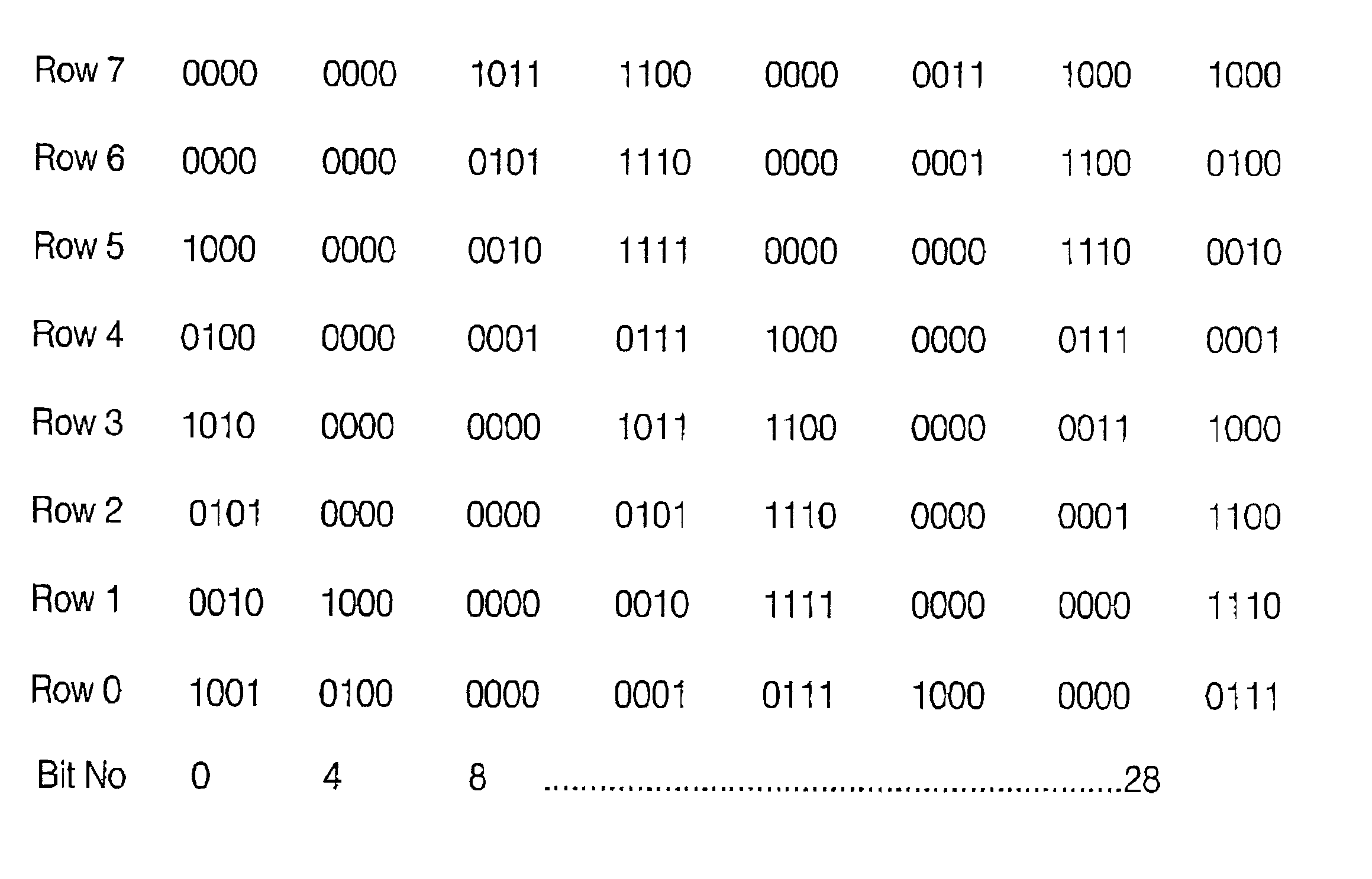
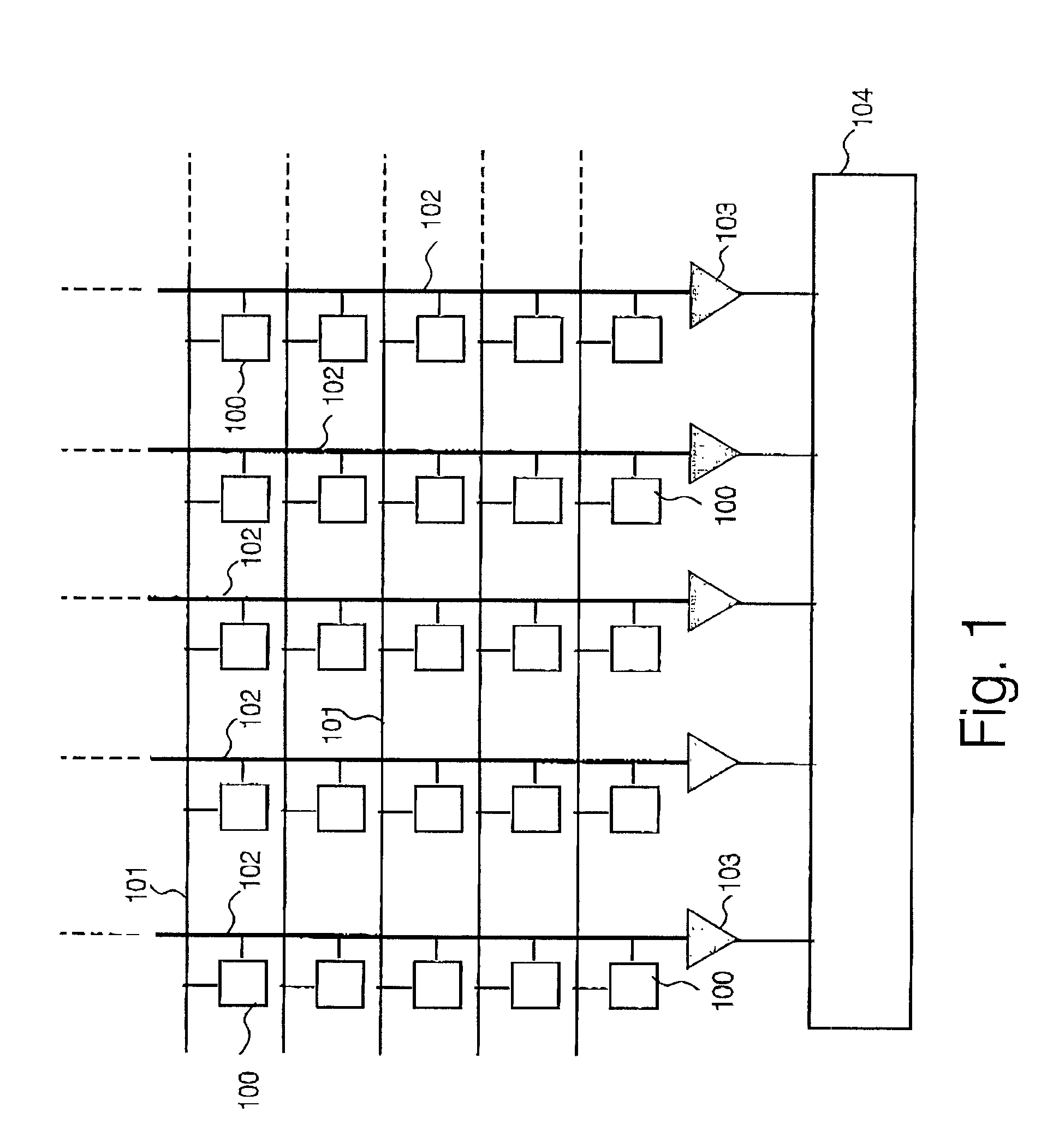
Referring to FIG. 1 herein, there is illustrated schematically a small area of a two-dimensional array of memory elements of a magnetic random access memory (MRAM). A plurality of memory elements 100 are arranged in a two-dimensional array in a plurality of rows and a plurality of columns. Along each row extends a corresponding respective word line 101 and along each column extends a corresponding respective bit line 102, each memory elemen...


PUM


Abstract

A data storage device comprises at least one array of memory elements arranged in a plurality of rows and columns; coding means for coding an input data into a form having a balanced proportion of "1's and "0's, said coding means comprising means for applying an output of a pseudo random bit sequence generator to said incoming data, wherein the coded data is stored in the array of memory elements such that the "1's and "0's are spatially distributed relatively evenly across the plurality of memory elements; and decoding means for decoding the coded data read from the plurality of memory elements, into the original data.

Description

The present invention relates to solid state data storage devices, and particularly although not exclusively, to solid state storage devices having one or more two-dimensional arrays of memory elements.BACKGROUND TO THE INVENTIONThe invention relates to solid state memory devices such as existing semi conductor technologies, for example dynamic random access memory (DRAM), FLASH and static random access memory (SRAM) or other technologies, for example magnetic random access memory (MRAM). In these devices, memory cells are arranged in one or more two-dimensional arrays addressed by word lines (rows) and bit lines (columns). To read and write cells in the arrays, one row and one or more bit lines are `selected` to access the required cells. Depending upon the implementation, there may be one read / write circuit per column (enabling all bits on the row to be read / written simultaneously) or read / write circuits may be multiplexed or shared between columns.In DRAM, the memory cell uses a ...

Claims


Application Information

Patent Timeline
Patent Type & Authority Patents(United States)
IPC IPC(8): G11C7/10G11C11/16G11C11/02
CPCG11C11/16G11C7/1006G11C11/1675
Inventor MORLEY, STEPHENLLOYD-JONES, KEVINMCCARTHY, DOMINIC P.BRAMHALL, PETER JOSEPH
Owner SAMSUNG ELECTRONICS CO LTD
Why Eureka
Try Eureka