
Nonvolatile memory device and related method of operation

a nonvolatile memory and device technology, applied in the field of electronic memory technologies, to achieve the effect of improving the performance and reliability of nonvolatile memory devices

Active Publication Date: 2013-10-31
SAMSUNG ELECTRONICS CO LTD
View PDF4 Cites 29 Cited by
  • Summary
  • Abstract
  • Description
  • Claims
  • Application Information

AI Technical Summary

Benefits of technology

The patent text discusses a way to make nonvolatile memory devices better by improving their performance and reliability. This is done by addressing the problems caused by electrical disturbances between different memory cells. The technical effect of this invention is that it can make nonvolatile memory devices more robust and reliable.

Problems solved by technology

Nevertheless, the development of the 3D array technology has presented a number of technical challenges and opportunities to be addressed through ongoing innovation.

Method used


Image

  • Nonvolatile memory device and related method of operation
  • Nonvolatile memory device and related method of operation
  • Nonvolatile memory device and related method of operation

Examples


Embodiment Construction

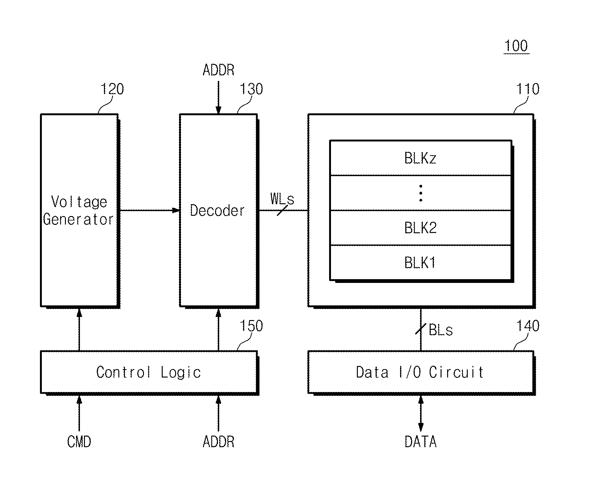
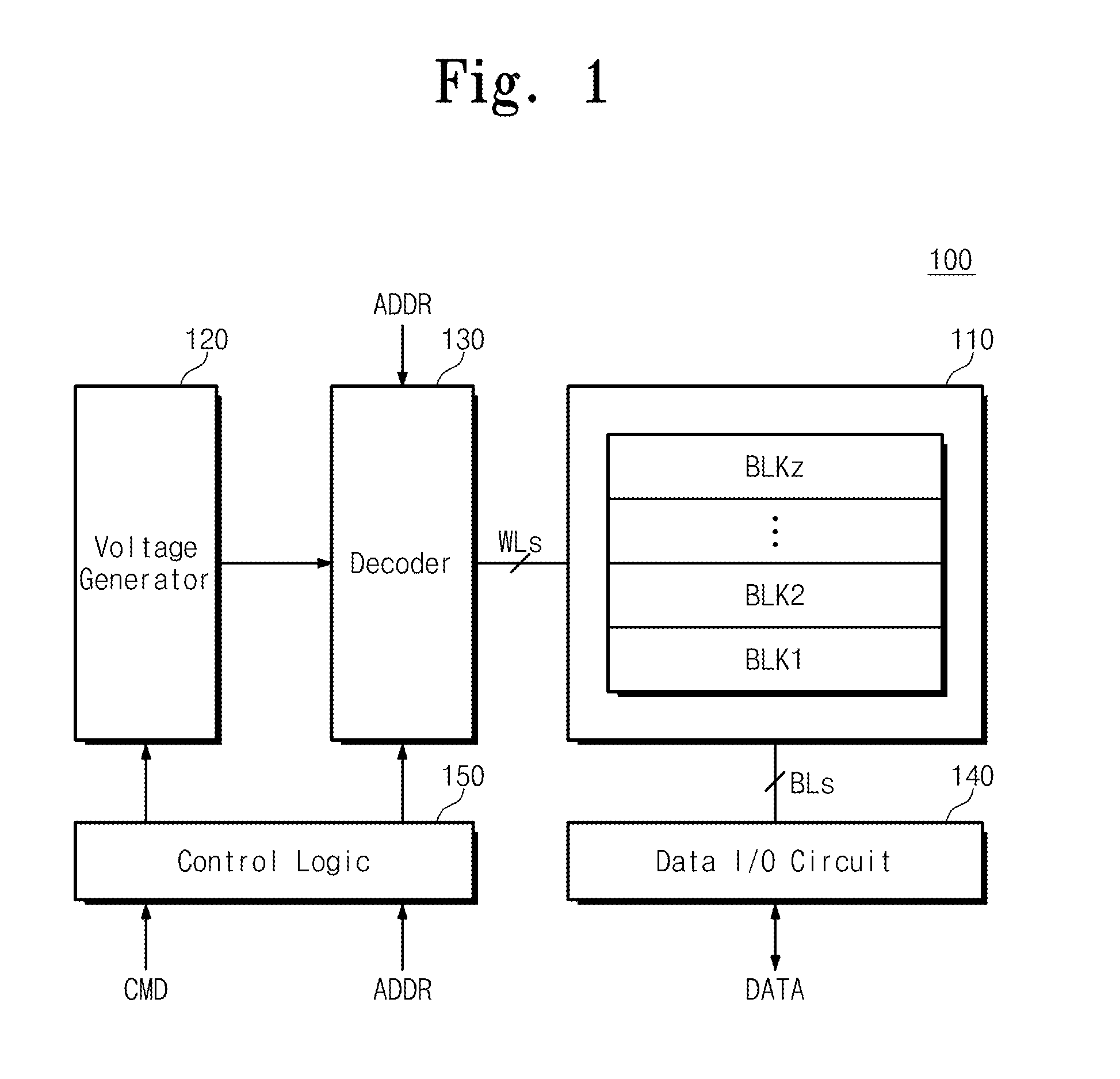
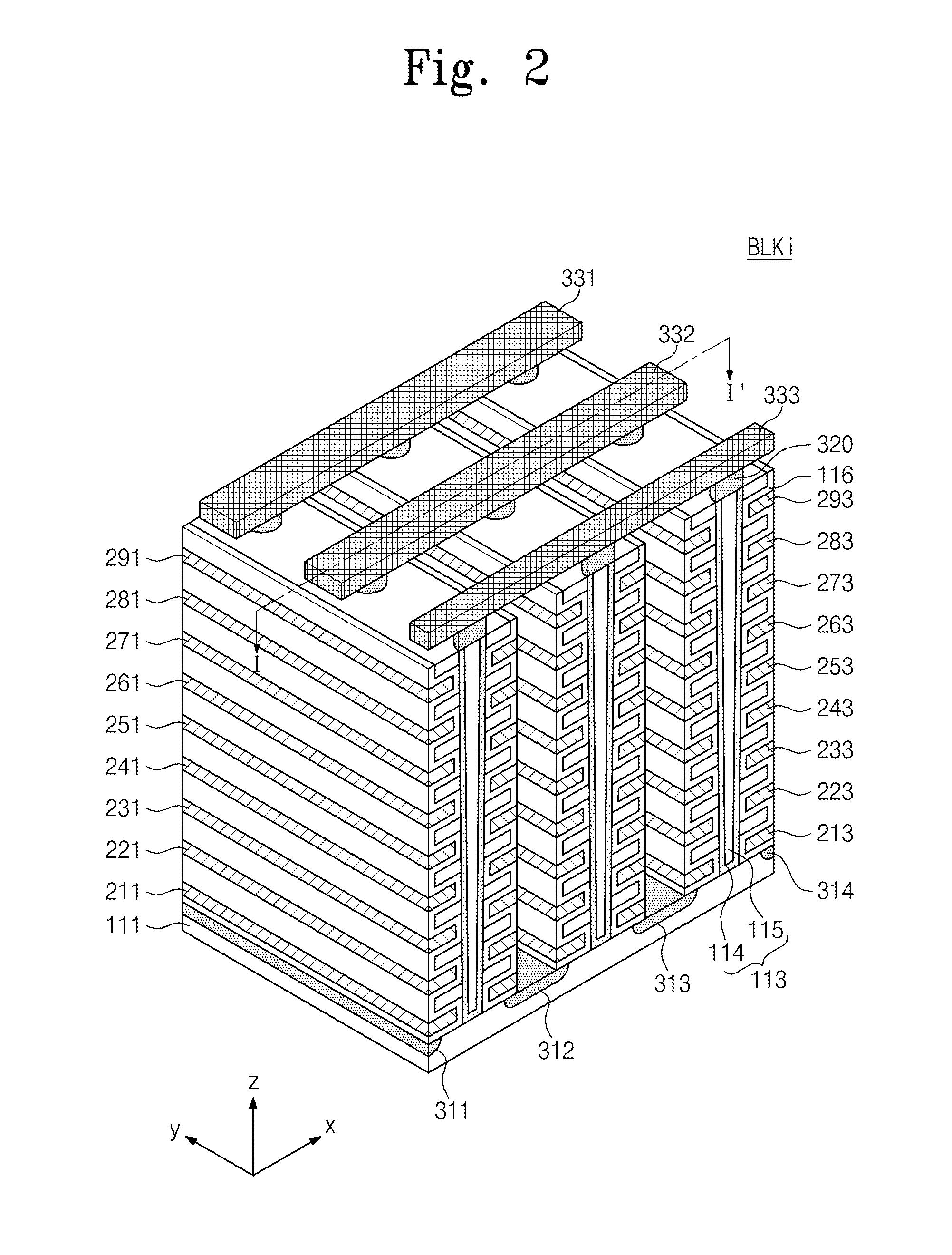
[0034]Embodiments of the inventive concept are described below with reference to the accompanying drawings. These embodiments are presented as teaching examples and should not be construed to limit the scope of the inventive concept.

[0035]In the description that follows, the terms “first”, “second”, “third”, etc., may be used to describe various features, but the described features should not be limited by these terms. Rather, these terms are used merely to distinguish between different features. Thus, a first feature could alternatively be termed a second feature and vice versa without materially altering the meaning of the relevant description.

[0036]Spatially relative terms, such as “beneath”, “below”, “lower”, “under”, “above”, “upper” and the like, may be used for ease of description to describe spatial relationships between different features as illustrated in the drawings. The spatially relative terms are intended to encompass different orientations of the device in use or ope...


PUM


Abstract

A nonvolatile memory device comprises cell strings formed in a direction substantially perpendicular to a substrate and is configured to select memory cells in units corresponding to a string selection line. The device selects a page to be programmed among pages sharing a common word line, determines a level of a program voltage to be provided to the selected page according to a location of a string selection line corresponding to the selected page, and writes data in the selected page using the determined level of the program voltage.

Description

CROSS-REFERENCE TO RELATED APPLICATIONS[0001]This application claims priority under 35 U.S.C. §119 to Korean Patent Application No. 10-2012-0043887 filed on Apr. 26, 2012, the subject matter of which is hereby incorporated by reference.BACKGROUND OF THE INVENTION[0002]The inventive concept relates generally to electronic memory technologies. More particularly, certain embodiments of the inventive concept relate to nonvolatile memory devices and related methods of operation.[0003]Semiconductor memory devices can be roughly divided into two categories according to whether they retain stored data when disconnected from power. These categories include volatile memory devices, which lose stored data when disconnected from power, and nonvolatile memory devices, which retain stored data when disconnected from power. Examples of volatile memory devices include static random access memory (SRAM) and dynamic random access memory (DRAM). Examples of nonvolatile memory devices include masked re...

Claims


Application Information

Patent Timeline
Patent Type & Authority Applications(United States)
IPC IPC(8): G11C16/10G11C16/34
CPCG11C16/10G11C16/34G11C11/5628G11C11/5642G11C16/0483G11C16/3427G11C2211/5621H10B69/00H10B41/27H10B43/27
Inventor KWAK, DONGHUN
Owner SAMSUNG ELECTRONICS CO LTD
Learn More