Group III nitride compound semiconductor device
a semiconductor device and nitride technology, applied in the direction of semiconductor laser structure details, semiconductor lasers, nanoinformatics, etc., can solve the problems of easy generation of dislocations, poor device characteristics of fabricated devices, and drawbacks of above-mentioned conventional semiconductors
- Summary
- Abstract
- Description
- Claims
- Application Information
AI Technical Summary
Benefits of technology
Problems solved by technology
Method used
Image

Examples
first embodiment
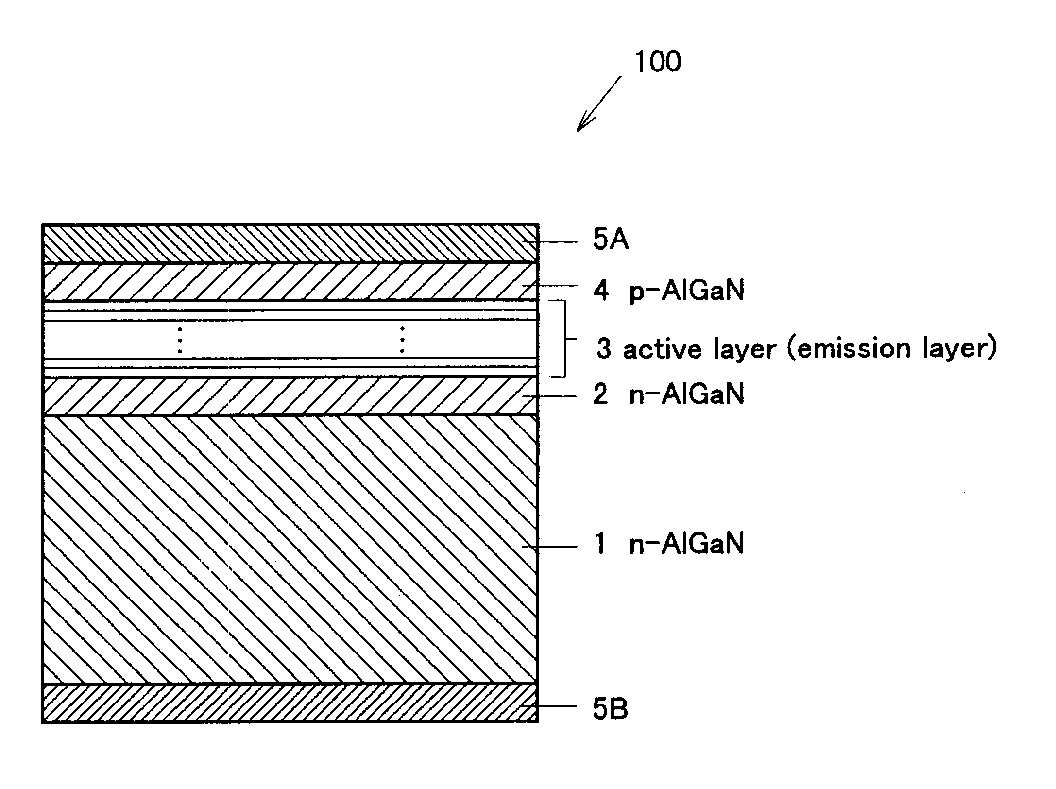
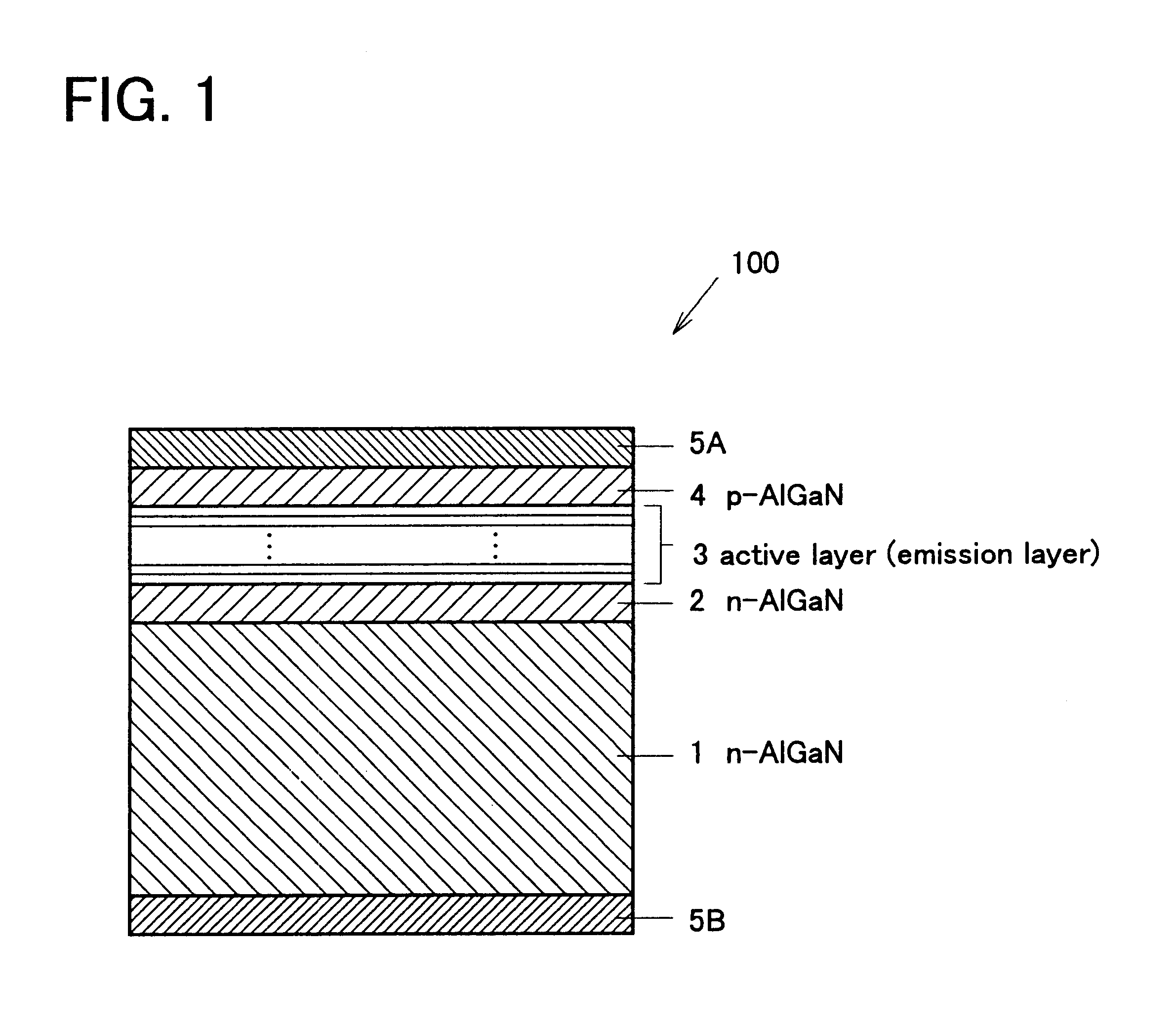
A light-emitting diode 100 having a structure shown in FIG. 1 was produced. The LED 100 contains an n-type Al.sub.0.07 Ga.sub.0.93 N substrate 1 having a thickness of approximately 100 .mu.m and an electron density of 3.times.10.sup.17 / cm.sup.3.
The following layers were formed on the n-type Al.sub.0.07 Ga.sub.0.93 N substrate 1, in the order presented, an Si-doped Al.sub.0.07 Ga.sub.0.93 N n-type cladding layer 2 having a thickness of approximately 0.5 .mu.m and an electron density of 2.times.10.sup.18 / cm.sup.3 ; a GaN active layer 3 having a thickness of 50 nm; an Mg-doped Al.sub.0.07 Ga.sub.0.93 N p-type cladding layer 4 having a thickness of approximately 0.5 .mu.m and a hole density of 5.times.10.sup.17 / cm.sup.3. A metal electrode 5A was formed on the cladding layer 4, and a metal electrode 5B was formed on the entire backside of the n-type Al.sub.0.07 Ga.sub.0.93 N substrate 1.
The metal electrode 5A, serving as a positive electrode, was formed from gold (Au). Alternatively, ...
second embodiment
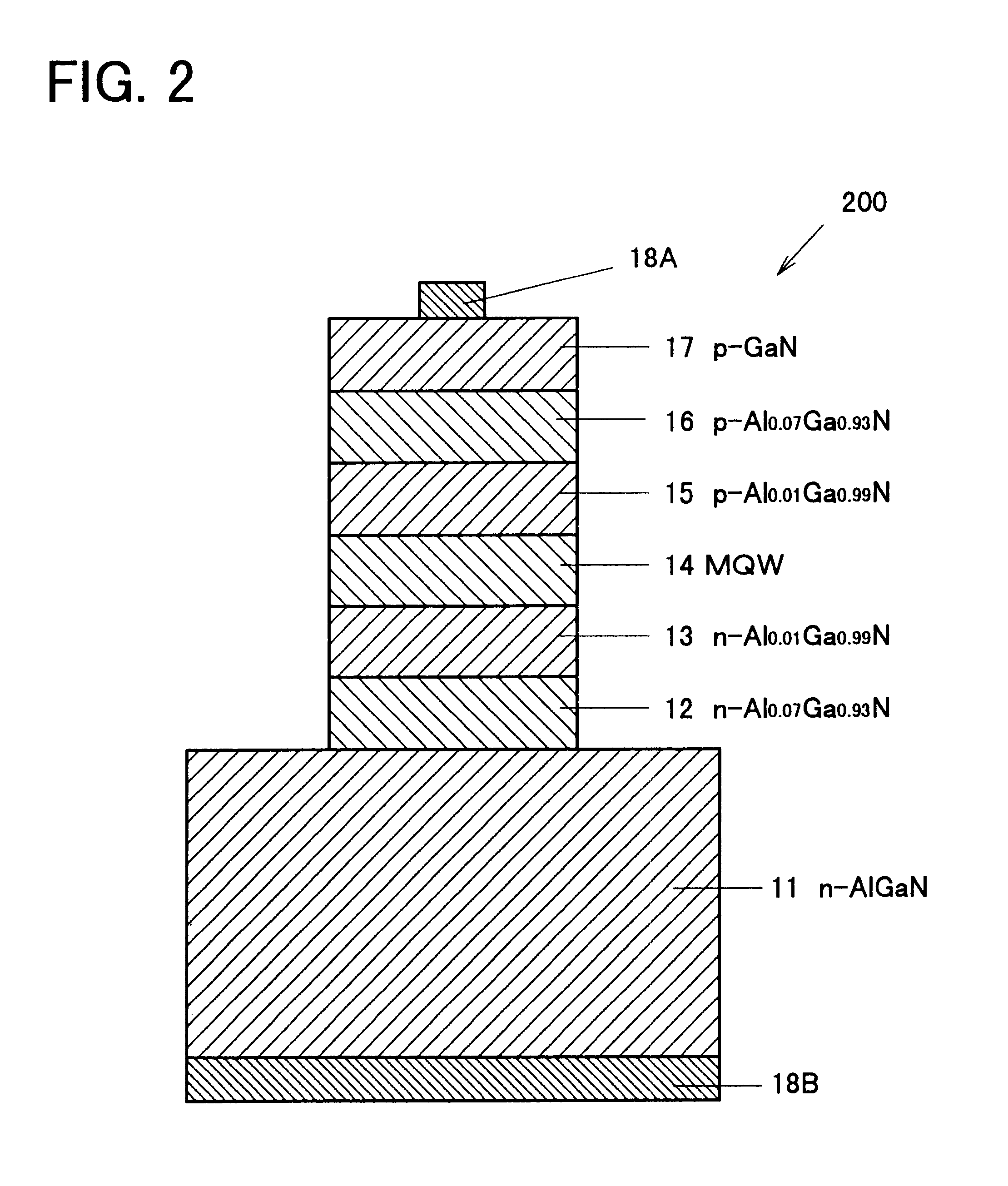
A laser diode 200 having a structure shown in FIG. 2 was produced. The LD 200 contains an n-type Al.sub.0.07 Ga.sub.0.93 N substrate 11 having a thickness of approximately 100 .mu.m and an electron density of 3.times.10.sup.17 / cm.sup.3.
On the n-type Al.sub.0.07 Ga.sub.0.93 N substrate 11 were formed, in the order given, an Si-doped Al.sub.0.07 Ga.sub.0.93 N n-type cladding layer 12 having a thickness of approximately 3 .mu.m and an electron density of 2.times.10.sup.18 / cm.sup.3 ; an Si-doped Al.sub.0.01 Ga.sub.0.99 N n-type guide layer 13 having a thickness of approximately 0.5 .mu.m and an electron density of 5.times.10.sup.17 / cm.sup.3 ; an emission layer 14 of a multiple quantum well (MQW) structure comprising five GaN well layers each having a thickness of 2 nm stacked alternately with six Al.sub.0.01 Ga.sub.0.99 N barrier layers each having a thickness of 5 nm; an Mg-doped Al.sub.0.01 Ga.sub.0.99 N p-type guide layer 15 having a thickness of approximately 0.5 .mu.m and a hole...
PUM
 Abstract
Description
Claims
Application Information
 - R&D Engineer
- R&D Manager
- IP Professional
- Industry Leading Data Capabilities
- Powerful AI technology
- Patent DNA Extraction
Browse by: Latest US Patents, China's latest patents, Technical Efficacy Thesaurus, Application Domain, Technology Topic.
© 2024 PatSnap. All rights reserved.Legal|Privacy policy|Modern Slavery Act Transparency Statement|Sitemap