Crosspoint switch with switch matrix module

a cross-switch and matrix module technology, applied in the field of integrated circuits, can solve the problems of limiting the number of inputs and outputs available, requiring reconfiguration of between outputs and inputs, increasing die area, heat generation,

Inactive Publication Date: 2005-09-20
MICROSEMI STORAGE SOLUTIONS
View PDF52 Cites 65 Cited by
  • Summary
  • Abstract
  • Description
  • Claims
  • Application Information

AI Technical Summary

Benefits of technology

[0020]The network includes series capacitors, and a combination of series resistors and shunt resistors, arranged such that the gain of the circuit is less than unity at low frequencies and rises with increasing frequency above a frequency determined by the desired maximum frequency of operation.
[0021]These and other aspects of the present invention will be more readily appreciated upon review of the following discussion and in view of the accompanying figures.

Problems solved by technology

Moreover, as nodes are often in communication with a number of other nodes, the connections between outputs and inputs often require reconfiguration during operation of the switch.
Increasing the numbers of inputs and outputs to a switch generally results in increased die area, power usage, heat generation, and complexity of the switch.
In many cases these constraints limit the number of inputs and outputs available on a particular integrated circuit forming a switch.
Generally, a three stage Clos network and a Benes network are more efficient in terms of minimizing the number of switch devices (N3 / 2 and NlogN respectively) but may be more complex in programming or scalability.
The use of a number of switch devices, however, is also problematic as the number of devices increases, with accompanying power and heat issues.
Larger switch size also sometimes increases the possibility of improper design or improper manufacturer of the chip.
Testing of larger switches, however, can at times be difficult, both with respect to internal switch operation as well as connections to the switch.
Absent adequate testing capability of the switch itself, determination of whether a particular chip is bad or whether connections to the chip are flawed may be difficult.
Further, larger switches require increased programming when determining the output input connections.
Indeed, in an extreme case operation of the switch may be delayed while continued programming of the switch occurs.
In addition, particularly at higher frequencies, data degradation may occur due to inter-symbol interference.
Inter-symbol interference (ISI) can result when the bandwidth of a transmission media or an amplifying circuit is not sufficient to pass the frequency content of a data signal without attenuating or phase-shifting some of the constituent frequencies such that a data pulse will not reach its full amplitude.
A signal that has been distorted in this way is difficult to recover error-free.
However, this is often not feasible where numerous amplifiers in a chain are required to accomplish a signal processing function.
Power dissipation constraints or capacitive loading conditions also limit the feasibility designing an amplifier to prevent ISI.
However, it is not always possible to have adequate bandwidth in a chain of amplifiers and meet other design constraints simultaneously.
Amplifiers with high bandwidth tend to dissipate more power and require more expensive IC processes.
If there is excess gain in the amplifier chain, negative feedback could be used to reduce gain and increase bandwidth, but this is not feasible if the output is not in proximity to the input.
Longer distances for the feedback path can result in delays that de-stabilize the feedback loop and cause it to oscillate.
This situation often occurs in un-retimed (asynchronous) cross-point switch circuits.
Hence, a significant delay would result to cause the circuit to oscillate undesirably.
Furthermore, an equalization approach generally cannot be applied at the output of a chain of limiting amplifiers, because some of the original characteristics of the signal have been removed by the limiting operation.

Method used


Image

  • Crosspoint switch with switch matrix module
  • Crosspoint switch with switch matrix module
  • Crosspoint switch with switch matrix module

Examples


Embodiment Construction

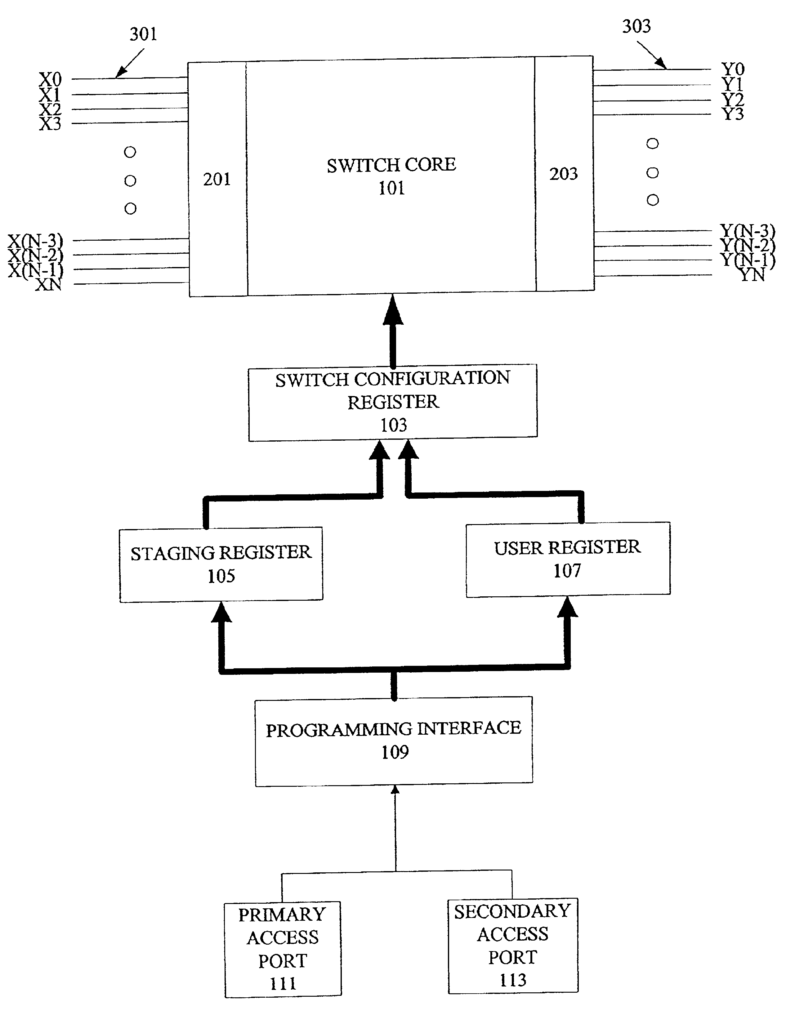
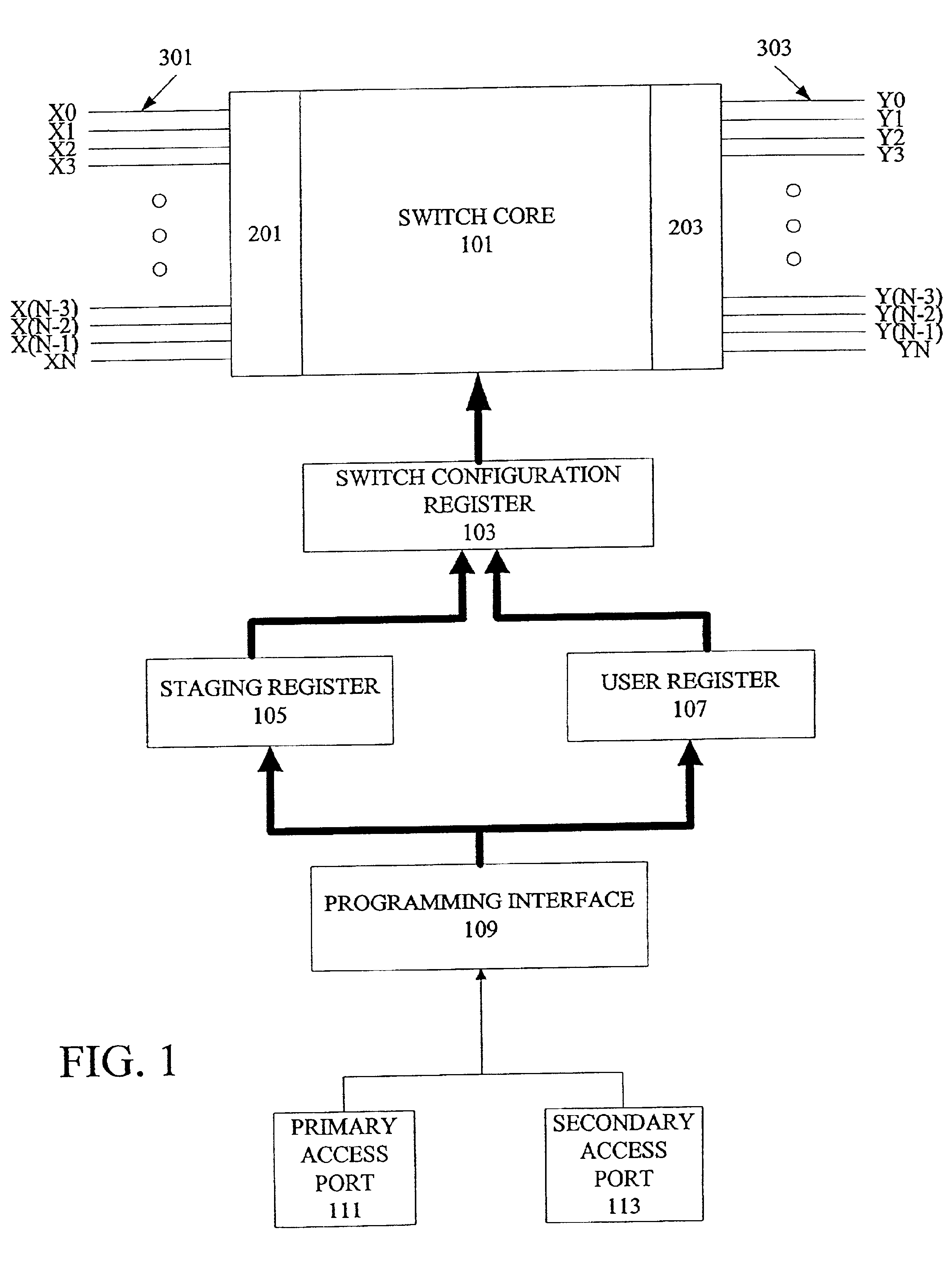
[0037]FIG. 1 illustrates a block diagram of one embodiment of a switch of the present invention. The switch includes a switch core 101, a switch configuration register 103, a staging register 105, and a programming interface 109. In somewhat more detail, the switch core couples signals from an input bus 301 to an output bus. The switch configuration register determines which output signals of the output bus are derived from which signals of the input bus. The staging register provides a temporary programming register, the contents of which are transferred to the switch configuration register when remapping of the outputs to the inputs is desired. The staging register is accessed using the programming register. The input bus provides a number of signals each to input signal equalization circuits 201. The input equalization circuits are coupled to the switch core. Similarly, outputs of the switch core are coupled to output level control circuits 203 which are coupled to an output bus ...


PUM


Abstract

A crosspoint switch including a switch matrix modules and programming features. A switch matrix modules include input lines tied to inputs of the switch through precompensation networks. The programming features include user initialization states and reduced and grouping command configuration operations.

Description

CROSS REFERENCE TO RELATED APPLICATIONS[0001]This application claims the benefit of the filing dates of U.S. Provisional Application entitled Switch Matrix Module (Application No. 60 / 209,552) filed on Jun. 6, 2000, and U.S. Provisional Application entitled Pre-Compensation System and Method For Reducing Inter-Symbol Interference (Application No. 60 / 227,550) of which are hereby incorporated by reference as if set forth in full herein.BACKGROUND OF THE INVENTION[0002]The present invention relates generally to integrated circuits, and more particularly to cross switches.[0003]Cross switches are often used to route data from a variety of inputs to a variety of outputs. With ever-increasing data communication needs, the number of inputs and outputs to cross switches has often been subject to increase. Moreover, as nodes are often in communication with a number of other nodes, the connections between outputs and inputs often require reconfiguration during operation of the switch.[0004]Inc...

Claims


Application Information

Patent Timeline
Patent Type & Authority Patents(United States)
IPC IPC(8): H01L23/02H01L23/48H04Q1/00G02B6/35H04Q3/52G06F13/40H01L23/538H04L12/56
CPCG06F13/4022H01L23/5382H04L49/65H01L2924/3011H04L49/101H01L2224/16225H01L2924/15311
Inventor MCCORMACK, GARYKYLES, IAN A.MCCAMANT, ANGUS J.SEITZ, NORBERT J.SUTER, RICHARD R.
Owner MICROSEMI STORAGE SOLUTIONS
Why Eureka
Try Eureka