Liquid-crystal display
Inactive Publication Date: 2003-04-22
CITIZEN WATCH CO LTD
16 Cites 76 Cited by
AI-Extracted Technical Summary
Problems solved by technology
With such a reflection-type liquid crystal display device, however, external light passes through each of two sheets of the polarizing films twice from the time when the external light enters from the visible side of the device until it goes out towards the visible side after reflected by a reflector, so that reduction in light quantity is increased, thereby lowering brightness of images in display.
Moreover, since the reflector is installed on the outer side of a glass substrate of the liquid crystal element, there has arisen a problem that shadows appear on display.
With such a conventional single polarizing film type liquid crystal display device as described above, however, a problem has been encountered that excellent black display can not be effected, and contrast becomes low.
However, with the single polarizing film type liquid crystal display device, employing one sheet of retardation film described above, a low reflectance can be achieved for l...
Abstract
A reflection-type liquid crystal display device of single polarizing film type, comprises a liquid crystal element (20) comprised of twisted nematic liquid crystal (6) sandwiched between a first substrate (1) provided with a reflector (7) and first electrodes (3), and a second substrate (2) provided with second electrodes (4), and a twisted retardation film (12), a first retardation film (13), a second retardation film (14), a polarizing film (11) that are disposed in sequence on the outer side of the second substrate (2), so that black display having a low reflectance is obtained over the all-wavelength region, thereby effecting bright display in high contrast.
Application Domain
Static indicating devicesNon-linear optics
Technology Topic
High contrastReflectivity +5
Image
Examples
- Experimental program(8)
Example
A first embodiment of 
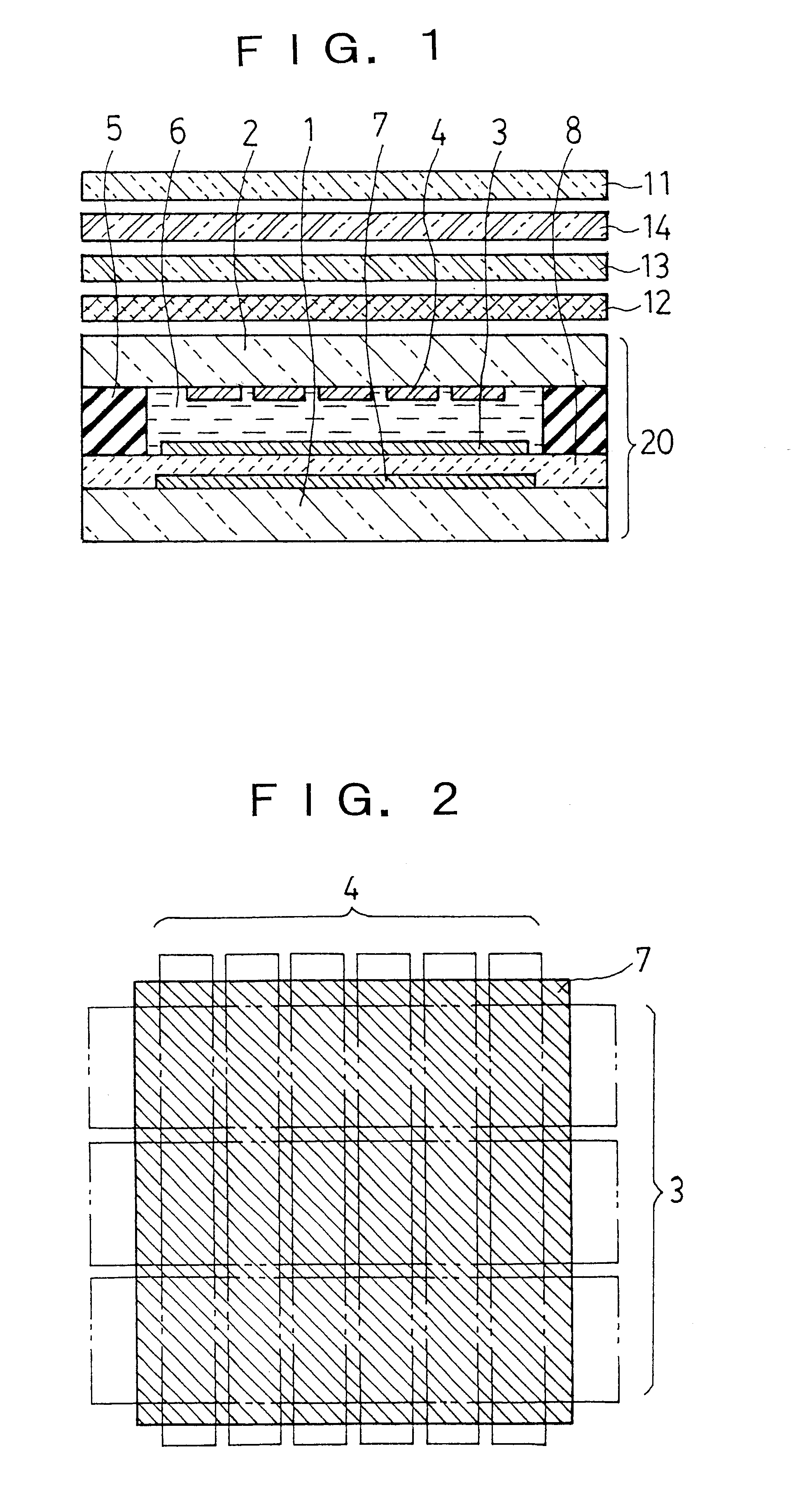
a liquid crystal display device according to the invention is described with reference to FIGS. 1 and 2.
FIG. 1 is a schematic sectional view showing the constitution of the liquid crystal display device, and FIG. 2 is a plan view showing a planar layout relationship among a reflector, first electrodes, and second electrodes, installed in the device.
As shown in FIG. 1, the liquid crystal display device is comprised of a liquid crystal element 20, and a twisted retardation film 12, a first retardation film 13, a second retardation film 14, and a polarizing film 11 that are disposed in sequence on the outer side (a side opposite from the side facing nematic liquid crystal: the visible side) of a second substrate 2 of the liquid crystal element 20, thereby constituting a reflection-type liquid crystal display device of single polarizing fil-type.
The polarizing film 11, the second retardation film 14, the first retardation film 13, and the twisted retardation film 12 are integrally bonded with each other by use of an acrylic adhesive, and are pasted to the outer face of the second substrate 2 of the liquid crystal element 20 by use of an acrylic adhesive.
The liquid crystal element 20 is comprised of: a first substrate 1 and the second substrate 2, made up of a glass sheet 0.5 mm thick, respectively, and bonded with each other at the periphery thereof with a sealant 5; and nematic liquid crystal 6 aligned so as to be twisted through 240 degrees left-handed and sealed in a gap formed therebetween to be held therein-between.
On the inner face of the first substrate 1, a reflector 7 made of aluminum 0.2 .mu.m thick, and a protective film 8 made of an acrylic material 2 .mu.m thick, covering the reflector 7, are formed, and first electrodes 3 are formed further on top of the protective film 8.
On the inner face of the second substrate 2, second electrodes 4 are formed. Both the first electrodes 3 and the second electrodes 4 are made up of an indium tin oxide (ITO) film which is a transparent and electrically conductive film, and are patterned in a multitude of stripes in such a way as to cross each other at right angles, as shown in FIG. 2. Spots where the first electrodes 3 and the second electrodes 4 cross and superpose each other, respectively, constitute respective pixels. An alignment film (although not shown) is formed on the protective film 8 of the first substrate 1 with the first electrodes 3 formed thereon, and on the inner face of the second substrate 2 with the second electrodes 4 formed thereon, respectively.
Transmittance of the first electrodes 3 and the second electrodes 4, made up of the ITO film, is important in respect of brightness. The lower a sheet resistance value of the ITO film, the thicker the thickness of the film becomes, thereby lowering transmittance.
With this embodiment, data signals are applied to the second electrodes 4, and accordingly, an ITO film having a sheet resistance value at about 100 ohms, and a thickness in the order of 0.05 .mu.m is used for the second electrodes 4 so that the effect of cross talk can be reduced. An average transmittance of the ITO film is about 92%.
Further, scanning signals are applied to the first electrodes 3, and accordingly, an ITO film having a sheet resistance value at about 10 ohms, and a thickness in the order of 0.3 .mu.m is used for the first electrodes 3 in order to reduce cross talk. An average transmittance of the ITO film is a little lower at about 89%, however, brightness of images in display can be improved by use of a transparent electrode having a transmittance at 90% or more for at least one of the electrodes.
The twisted retardation film 12 is a film made of a liquid crystalline high polymer of a twist structure, applied to a triacetyl cellulose (TAC) film or a polyethylene telephthalate (PET) film after an alignment treatment, rendered into liquid crystal state at a high temperature of about 150.degree. C., and rapidly cooled to room temperature after adjustment of a twist angle so as to fix a twist condition thereof.
Otherwise, the twisted retardation film 12 may be formed by transferring a liquid crystalline high polymer with a fixed twist condition thereof to a TAC film which is separately prepared and to which an alignment layer treatment has been applied.
With this embodiment, the twisted retardation film 12 having a twist angle Tc at -240.degree., a .DELTA.nd value Rc, indicating a birefringent tendency, at 0.80 .mu.m, and a right-handed twist direction is used.
The polarizing film 11 is preferably as bright as possible, and its polarization degree is preferably as high as possible. With this embodiment, material having a polarization degree of 99.9% at a transmittance of 45% is used for the polarizing film.
If an anti-reflection layer having a reflectance in the order of 0.5% is provided by coating the surface of the polarizing film 11 with inorganic thin films in a plurality of layers, differing in reflectance, by use of the vapor deposition method or the sputtering method, surface reflectance of the polarizing film 11 is lowered and transmission is improved so that brightness of images is enhanced. Also, since a blackness level is lowered, contrast is improved as well.
However, since the inorganic thin films is expensive, there has been developed a coat-type anti-reflection layer coated with an organic material in one to two layers. Such an anti-reflection layer has a somewhat high reflectance around 1%, however, its price is low. The above-described anti-reflection layer is good enough for use as the anti-reflection layer of the liquid crystal display device.
The first retardation film 13 is a transparent film about 70 .mu.m thick, formed by drawing polycarbonate (PC), and has a retardation value F1 of 0.36 .mu.m at a wavelength of 0.55 .mu.m.
The second retardation film 14 is a transparent film about 100 .mu.m thick, formed by drawing polypropylene (PP), and has a retardation value F2 of 0.50 .mu.m at a wavelength of 0.55 .mu.m.
Hereinafter, a layout relationship among respective constituent members is described with reference to FIGS. 3 and 4.
An alignment film (not shown) is formed on the surface of the first electrodes 3 as well as the second electrodes 4 of the liquid crystal element 20, and as shown in FIG. 3, a lower molecular alignment direction 6a of the nematic liquid crystal 6 points at +30.degree. by applying a rubbing treatment to the inner face of the first substrate 1 in the direction extending upward to the right at 30.degree. to the horizontal axis while an upper molecular alignment direction 6b of the nematic liquid crystal 6 points at -30.degree. by applying a rubbing treatment to the inner face of the second substrate 2 in the direction extending downward to the right at 30.degree. to the horizontal axis. Generally, an angle of clockwise rotation is expressed in minus, and an angle of counterclockwise rotation is expressed in plus.
The liquid crystal element 20 of STN mode, having a twist angle Ts of 240.degree. counterclockwise, is made up by adding an optical rotatory substance called chiral to the nematic liquid crystal 6 having a viscosity at 20 cp, and adjusting a twist pitch P to 11 .mu.m.
A birefringence difference .DELTA.n of the nematic liquid crystal 6 is set at 0.15, and a cell gap d which is a gap between the first substrate 1 and the second substrate 2 is set at 5.6 .mu.m. Accordingly, a .DELTA.nd value Rs indicating the birefringent tendency of the liquid crystal element 20 as expressed by the product of the birefringence difference .DELTA.n of the nematic liquid crystal 6 and the cell gap d becomes 0.84 .mu.m.
The polarizing film 11 is disposed such that a transmission axis 11a thereof forms an angle of +45.degree. on the basis of the horizontal axis.
As shown in FIG. 4, a lower molecular alignment direction 12a of the twisted retardation film 12 is +60.degree. on the basis of the horizontal axis, and an upper molecular alignment direction 12b thereof is -60.degree. on the basis of the horizontal axis. Accordingly, the twist direction of the twisted retardation film 12 is clockwise, and a twist angle Tc thereof becomes -240.degree.. Assuming that a difference in absolute value between the twist angle of the liquid crystal element 20 and that of the twisted retardation film 12 is .DELTA.T, .DELTA.T=.vertline.Ts.vertline.-.vertline.Tc.vertline.=0.degree.. Further, a .DELTA.nd value Rc indicating the birefringent tendency of the twisted retardation film 12 is 0.80 .mu.m, and assuming that a difference with the .DELTA.nd value Rs of the liquid crystal element 20 is .DELTA.R, .DELTA.R=Rs-Rc=0.04 .mu.m.
That is, the twist direction of the twisted retardation film 12 is opposite to that of the liquid crystal element 20, and the twist angles of both are equivalent to each other (need only be substantially equivalent) while the .DELTA.nd values of both are substantially equivalent to each other as well.
As shown in FIG. 4, the first retardation film 13 is disposed such that a phase delay axis 13a thereof is oriented horizontally, and the second retardation film 14 is disposed such that a phase delay axis 14a thereof is oriented vertically, so that the phase delay axis 13a and the phase delay axis 14a cross each other at right angles.
Accordingly, the retardation value F1 of the first retardation film 13 and the retardation value F2 of the second retardation film are subjected to subtraction, so that an effective retardation value is .DELTA.F=F2-F1=0.14 .mu.m.
Advantageous effects of the liquid crystal display device according to the first embodiment are described hereinafter with reference to FIGS. 11 and 12 as well.
With the liquid crystal display device, as described in the foregoing, the twist angle Tc and the .DELTA.nd value Rc of the twisted retardation film 12 are set to be substantially equivalent to the twist angle Ts and the .DELTA.nd value Rs of the liquid crystal element 20, respectively, and further, as shown in FIG. 4, by disposing the twisted retardation film 12 such that the upper and lower molecular alignment directions 12b, 12a thereof are orthogonal to the lower and upper molecular alignment directions 6a, 6b of the liquid crystal element 20 shown FIG. 3, respectively, birefringent tendency that will occur in the liquid crystal element 20 will be fully compensated, thus preventing occurrence of birefringence.
In practice, since a tilt angle indicating an inclination of the molecules of the nematic liquid crystal 6 inside the liquid crystal element 20 is greater than a tilt angle of the twisted retardation film 12, it is preferable to set the .DELTA.nd value Rc of the twisted retardation film 12 to a value a little smaller than the .DELTA.nd value Rs of the liquid crystal element 20 from the viewpoint of fully compensating the birefringence described above.
Also, it is more preferable to match wavelength dependency of the refractive index of the liquid crystal molecules of the nematic liquid crystal 6 with wavelength dependency of the refractive index of liquid crystal polymer molecules of the twisted retardation film 12.
Even if the twist angle Tc of the twisted retardation film 12 differs from the twist angle Ts of the liquid crystal element 20, this allows the compensation to be effected to some extent.
The results of experiments showed that the compensation was effected when the twist angle Tc of the twisted retardation film 12 was within a range of the twist angle Ts (of the liquid crystal element 20) .+-.20.degree., but the compensation was best effected when Tc is substantially equivalent to Ts, and Tc is slightly larger than Ts.
FIG. 5 shows a relationship among the direction of phase delay axes 13a, 14a of the first and second retardation films and the upper molecular alignment direction 12b of the twisted retardation film 12 and the lower molecular alignment direction 12a thereof in the case where Tc=-245.degree., greater by 5.degree. in absolute value than Ts (240.degree.). In this case, optimum compensation was effected.
Then, the effect of the retardation films is described hereinafter. FIG. 11 shows wavelength dependency of retardation value of the retardation films used in carrying out this embodiment. The horizontal axis indicates light wavelengths (unit: .mu.m), and the vertical axis the retardation values (unit: .mu.m) of the retardation films.
In FIG. 11, curves 31, 32 indicate the retardation value of the first and second retardation films 13, 14, respectively, and a curve 33 indicates a retardation value when the second retardation film 14 is superposed on the first retardation film 13 such that respective phase delay axes cross each other at right angles.
Since the constituent material of the first retardation film 13 is polycarbonate (PC) having a large wavelength-dependency of refractive index, hence retardation values for light rays at short wavelengths undergo an increase as shown by the curve 31. On the other hand, the constituent material of the second retardation film 14 being polypropylene (PP) having a small wavelength-dependency of reflectance, retardation values for light rays at short wavelengths are substantially the same as those for light rays at long wavelengths, hardly undergoing any change as shown by the curve 32.
Accordingly, by superposing the second retardation film 14 on the first retardation film 13 such that the respective phase delay axes cross each other at right angles so as to decrease a retardation value, retardation values for light rays at short wavelengths around 0.4 .mu.m can be rendered smaller than those for light rays at long wavelengths around 0.7 .mu.m as shown by the curve 33.
Generally, linearly polarized light falling on a retardation film (quarter-wavelength film), having a retardation value equivalent to one quarter of light wavelength .lambda., with its polarization axis oriented at 45.degree. to the phase delay axis of the retardation film, can be converted into circularly polarized light.
Accordingly, with a configuration wherein a polarizing film, a quarter-wavelength film and a reflector are disposed so as to be superposed one after another in this order from the incident side of light, linearly polarized light falling through the polarizing film is turned into circularly polarized light at the quarter-wavelength film, is reflected at the reflector, and is transmitted through the quarter-wavelength film again, whereupon the direction of polarization is rotated through 90.degree., and the circularly polarized light reverts to linearly polarized light, which is absorbed by the polarizing film, thereby indicating black display.
With an ordinary quarter-wavelength film, however, since retardation values for light rays at short wavelengths are larger than those for light rays at long wavelengths, the quotient of a retardation value divided by a wavelength in the range of short wavelengths is larger than one quarter while the same in the range of long wavelengths is smaller than one quarter. As a result, perfect circularly polarized light can not be obtained, so that perfect black can not be indicated.
For this reason, as in this embodiment, by use of two sheets of the retardation films each having a different wavelength dependency of refractive index, it becomes possible to form a so-called wide-band quarter-wavelength film wherein retardation values in a short wavelength region are smaller than those in a long wavelength region. That is, the quotients of retardation values divided by wavelengths can be rendered approximately one quarter over the entire visible light region. Consequently, circularly polarized light can be obtained in all wavelength regions, so that perfect black in display can be obtained.
FIG. 12 shows reflection characteristics of the single polarizing film type liquid crystal display device according to this embodiment. A curve 34 indicates reflectance in a black display state when no voltage is applied between the first electrodes 3 and the second electrodes 4 inside the liquid crystal element 20, and a curve 35 indicates reflectance in a white display state when a predetermined voltage is applied. For the sake of comparison, a curve 36 indicates reflectance in a black display state of a single polarizing film type liquid crystal display device, wherein a quarter-wavelength film comprised of a single retardation film made of ordinary polycarbonate (PC) is used for a retardation film, when no voltage is applied. Herein, reflectance refers to a ratio (%) of an outgoing light quantity to an incident light quantity as seen from the visible side.
In FIG. 1, when no voltage is applied to the liquid crystal element 20, upon linearly polarized light falling through the polarizing film 11 from the upper visible side, components of the linearly polarized light at all wavelengths in the visible light region is turned into circularly polarized light after passing through the second retardation film 14 and the first retardation film 13. Since the twisted retardation film 12 and the liquid crystal element 20 are fully compensated, the circularly polarized light undergoes no change in polarization state, and arrives at the reflector 7 as it is. The circularly polarized light reflected at the reflector 7 undergoes no change even after passing through the liquid crystal element 20 and the twisted retardation film 12, however, when passing through the first retardation film 13 and the second retardation film 14, the circularly polarized light reverts to linearly polarized light with the direction of polarization rotated through 90.degree., and the linearly polarized light is nearly all absorbed by the polarizing film 11, so that display in perfect black with low reflectance as indicated by the curve 34 in FIG. 12 can be obtained.
If only a sheet of quarter-wavelength film made of ordinary polycarbonate (PC) is used instead of the first retardation film 13 and the second retardation film 14, light components in the short wavelength range as well as the long wavelength range are leaked, and perfect black display can not be effected, thereby indicating purplish black display, and lowering contrast.
Next, when a predetermined voltage is applied between the first electrodes 3 and the second electrodes 4 inside the liquid crystal element 20, the liquid crystal molecules of the nematic liquid crystal 6 are caused to rise, and a real .DELTA.nd value of the liquid crystal element 20 decreases.
Consequently, the linearly polarized light falling through the polarizing film 11 from the visible side is turned into the circularly polarized light after passing through the second retardation film 14 and the first retardation film 13, but reverts to elliptically polarized light or linearly polarized light as a result of passing through the twisted retardation film 12 and the liquid crystal element 20.
When birefringence occurring to the liquid crystal element 20 is equalized with that of the quarter-wavelength film by applying the voltage, the linearly polarized light falling through the polarizing film 11 as shown in FIG. 1 is not rotated even when reflected by the reflector 7 and passing through the twisted retardation film 12 and the liquid crystal element 20, thus returning as it is. Accordingly, all components thereof are transmitted through the polarizing film 11, and are sent out to the visible side, so that display in bright and excellent white at a high reflectance as indicated by the curve 35 in FIG. 12 can be obtained.
Thus, with the use of the polarizing film 11, the second retardation film 14, the first retardation film 13, the twisted retardation film 12, and the liquid crystal element 20 incorporating the reflector 7, it becomes possible to obtain display in excellent black and display in bright white, thereby enabling bright display in high contrast to be effected.
VARIATIONS OF THE FIRST EMBODIMENT
With the first embodiment described in the foregoing, an STN liquid crystal element twisted by 240 degrees is used for the liquid crystal element 20, however, even with the use of a TN liquid crystal element having a twist angle of around 90 degrees, a similar reflection-type liquid crystal display device of single polarizing film type can be obtained.
In the case of effecting a large screen display by use of the TN liquid crystal element, it is preferable to adopt an active-matrix reflection-type liquid crystal display device incorporating active elements such as TFTs, MIMs, and so forth.
Further, with this embodiment, a liquid crystalline polymer film in a fixed twist state at room temperature is used for the twisted retardation film 12, however, use of a temperature-compensation type twisted retardation film which is made only by bonding portions of liquid crystal molecules with polymer molecules in chain form, and having varying .DELTA.nd values (=Rc) thereof depending on temperature will improve brightness and contrast at high or low temperatures, so that a better reflection-type liquid crystal display device can be obtained.
With this embodiment, the reflector 7 is formed separately from the first electrodes 3, however, the first electrode may be formed of a metal such as aluminum, silver, and so forth, to be reflective electrodes doubling as the reflector 7. In this way, the device can be simplified in construction (the specific example thereof will be described hereinafter).
Further, the first substrate 1 need not be transparent. In the case of the first substrate 1 being transparent, even if the reflector 7 is disposed on the outer side of the first substrate 1, the substantially same effects can be obtained in respect of brightness and contrast although shadows occur to display.
Furthermore, with this embodiment, polycarbonate (PC) is used for the first retardation film 13, and polypropylene (PP) for the second retardation film 14, respectively, however, use of other constituent material may be effective to some extent as long as wavelength-dependencies of the refractive index of the respective retardation films differ from each other.
For example, in the case of using polyallylate for the first retardation film 13, and polyvinylalcohol for the second retardation film 14, good contrast was obtained.
Still further, with this embodiment, the retardation value F1 of the first retardation film 13 was set at 0.36 .mu.m, and the retardation value F2 of the second retardation film 14 at 0.50 .mu.m, however, provided that the relationship expressed by the formula, .DELTA.F=F2-F1=0.14 .mu.m, is maintained, the same effect can be obtained even if the retardation values F1, F2 differ from the values described above by way of example.
Example
SECOND EMBODIMENT
FIGS. 6 to 8
Now, a second embodiment of a liquid crystal display device according to the invention is described hereinafter with reference to FIGS. 6 to 8.
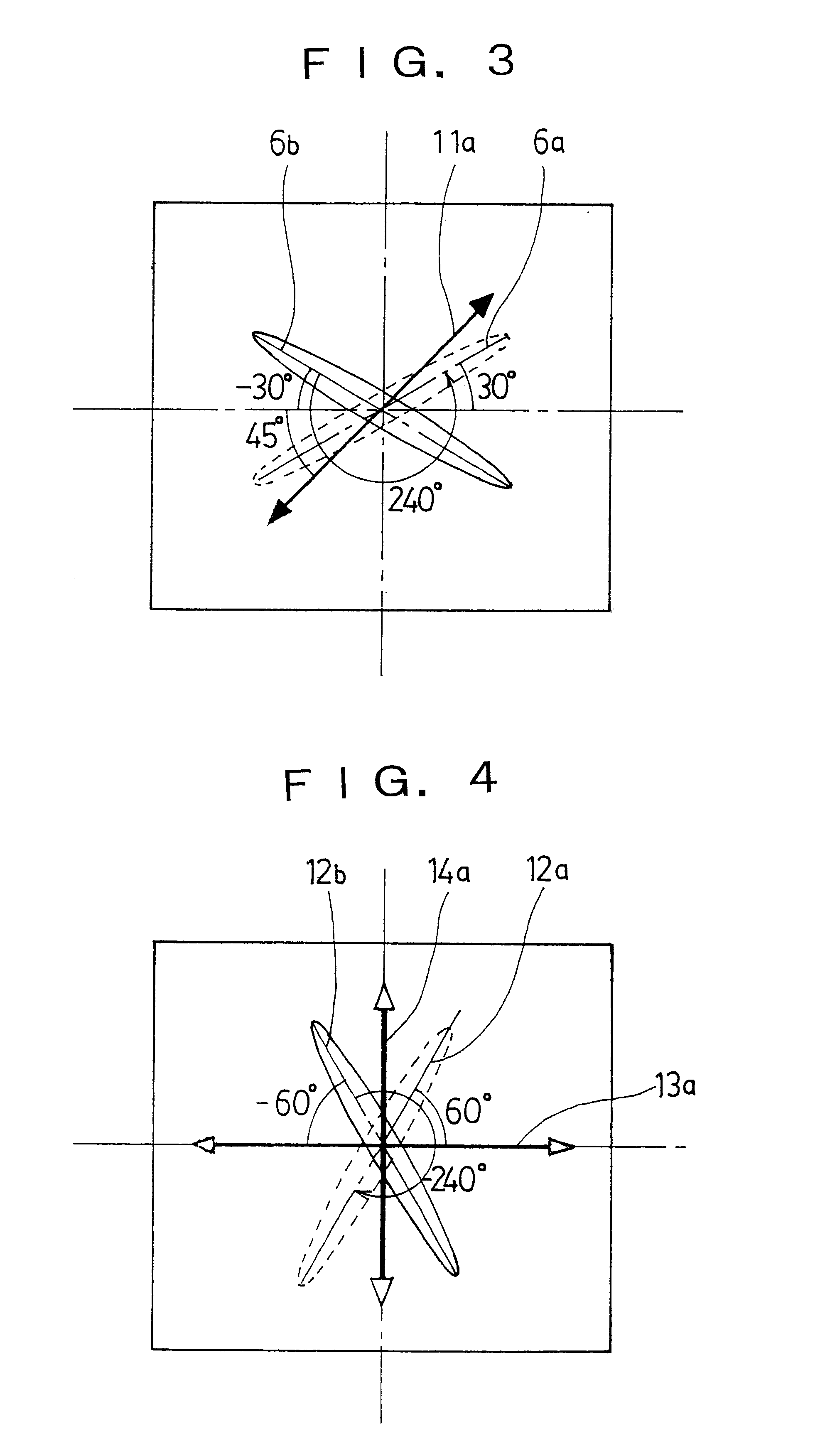
First, the configuration of the liquid crystal display device is described with reference to FIGS. 6 and 7. These figures are similar to FIGS. 1 and 2 for the first embodiment described above, and parts corresponding to those in FIGS. 1 and 2 are denoted by the like reference numerals. Description thereof is simplified or omitted.
The liquid crystal display device according to the second embodiment also constitutes a reflection-type liquid crystal display device of single polarizing film type, and differs from the constitution of the first embodiment of the invention only in respect of the type and installation angle of retardation films, installation of a diffusion film, use of reflective electrodes instead of the reflector.
A liquid crystal element 21 of the liquid crystal display device incorporates reflective electrodes 9 made of aluminum 0.2 .mu.m thick, formed directly on the inner face of a first substrate 1 thereof, and differs from the liquid crystal element 20 according to the first embodiment in that the reflector 7 and the protective film 8, shown in FIG. 1, are not installed.
The reflective electrodes 9 have the surface thereof serving as a reflection face, and serve as the first electrodes 3 and the reflector 7, shown in FIGS. 1 and 2. As shown in FIG. 7, the reflective electrodes 9 are patterned in stripes running in the direction orthogonal to second electrodes 4 which are transparent and patterned in stripes, and spots where the reflective electrodes 9 and the second electrodes 4 cross and superpose each other constitute respective pixels.
As shown in FIG. 6, on the outer side of a second substrate 2 of the liquid crystal element 21, a diffusion film 15, a twisted retardation film 12, a first retardation film 13, a second retardation film 14, and a polarizing film 11 are disposed in sequence, and the polarizing film 11, the second retardation film 14, the first retardation film 13, and the twisted retardation film 12 are integrally bonded with each other with an acrylic adhesive.
The diffusion film 15 is installed to obtain bright display having a wide viewing angle by scattering light rays reflected by the reflective electrodes 9.
Incident light rays entering from outside preferably undergo forward scattering as much as possible with less backward scattering because high contrast can be obtained in this way. In this case, a light scattering type adhesive 30 .mu.m thick, composed of fine particles mixed in an adhesive, is used for the diffusion film 15, and the light scattering type adhesive serves also as an adhesive for bonding of the diffusion film 15 with the second substrate 2 as well as the twisted retardation film 12.
The polarizing film 11 and the twisted retardation film 12 are the same as those used in the first embodiment.
The first retardation film 13 is a transparent film about 70 .mu.m thick, formed by drawing polycarbonate (PC), and has a retardation value F1=0.14 .mu.m, substantially equivalent to a quarter-wavelength at a wavelength of 0.55 .mu.m.
The second retardation film 14 is also a transparent film about 70 .mu.m thick, formed by drawing polycarbonate (PC), and has a retardation value F2=0.28 .mu.m, substantially equivalent to a half-wavelength at a wavelength of 0.55 .mu.m.
Hereinafter, a planar layout relationship of respective constituent members of the liquid crystal display device is described with reference to FIGS. 3 and 8.
An alignment film (not shown) is formed on the surface of the reflective electrodes 9 as well as the second electrodes 4 of the liquid crystal element 21, and as with the first embodiment shown in FIG. 3, a lower molecular alignment direction 6a of nematic liquid crystal 6, and an upper molecular alignment direction 6b of the nematic liquid crystal 6 points at +30.degree. and -30.degree. to the horizontal axis, respectively (an angle of counterclockwise rotation is expressed in plus, and an angle of clockwise rotation is expressed in minus).
The liquid crystal element 21 of STN mode, having a twist angle Ts of 240.degree. counterclockwise, is made up by adding an optical rotatory substance called chiral to the nematic liquid crystal 6 having a viscosity at 20 cp, and adjusting a twist pitch P to 11 .mu.m. A .DELTA.nd value Rs indicating the birefringent tendency of the liquid crystal element 21 is the same as that for the liquid crystal element 20, that is, 0.84 .mu.m.
The polarizing film 11 is disposed such that a transmission axis thereof forms an angle of +45.degree. on the basis of the horizontal axis as shown in FIG. 3.
As shown in FIG. 8, a lower molecular alignment direction 12a of the twisted retardation film 12 points at +60.degree. on the basis of the horizontal axis, and an upper molecular alignment direction 12b of molecules in the upper part thereof points at -60.degree. on the basis of the horizontal axis.
Accordingly, the twist direction of the twisted retardation film 12 is clockwise, and a twist angle Tc thereof becomes 240.degree.. Assuming that a difference in absolute value between the twist angle of the twisted retardation film 12 and that of the liquid crystal element 21 is .DELTA.T, .DELTA.T=.vertline.Ts.vertline.-.vertline.Tc.vertline.=0.degree.. Further, a .DELTA.nd value Rc indicating the birefringent tendency of the twisted retardation film 12 is 0.80 .mu.m, and assuming that a difference with the .DELTA.nd value Rs of the liquid crystal element 21 is .DELTA.R, .DELTA.R=Rs-Rc=(0.84-0.80) .mu.m=0.04 .mu.m, thus showing that the .DELTA.nd values of both are substantially equivalent to each other.
Further, as shown in FIG. 8, the phase delay axis 13a of the first retardation film 13 is disposed at -30.degree. on the basis of the horizontal axis while the phase delay axis 14a of the second retardation film 14 is disposed at +30.degree. on the basis of the horizontal axis.
Herein advantageous effects of the liquid crystal display device according to the second embodiment is described, however, effects of the twisted retardation film 12 and the liquid crystal element 21 are the same as those in the case of the first embodiment, that is, the former acting to fully compensate birefringent tendency occurring to the liquid crystal element 21. Accordingly, the advantageous effect of the retardation films only will be described hereinafter.
With the first embodiment, two sheets of the retardation films each having a different wavelength dependency of the refractive index thereof are used, however, even by use of two sheets of the retardation films having the same wavelength dependency of the refractive index, it is possible to obtain a wide-band quarter-wavelength film capable of converting light in the visible light range into circularly polarized light.
With the first embodiment, the second retardation film 14 is superposed on the first retardation film 13 such that respective phase delay axes cross each other at right angles, however, with the liquid crystal display device according to the second embodiment, the second retardation film 14 is superposed on the first retardation film 13 such that an angle of 60.degree. is formed between respective phase delay axes.
By superposing the second retardation film 14 having a retardation value F2=0.28 .mu.m substantially equivalent to a half-wavelength on the first retardation film 13 having a retardation value F1=0.14 .mu.m substantially equivalent to a quarter-wavelength such that an angle of 60.degree. is formed between the respective phase delay axes, a total retardation value for both the retardation films becomes 0.14 .mu.m at a wavelength of 0.55 .mu.m, but is less than 0.14 .mu.m at short wavelengths around 0.4 .mu.m, and greater than 0.14 .mu.m at long wavelengths around 0.7 .mu.m, and the effective phase delay axis becomes in the horizontal direction.
More specifically, by use of two sheets of the retardation films, even if each of them is made of material having the same wavelength-dependency of refractive index, it becomes possible to form a so-called wide-band quarter-wavelength film wherein retardation values in a short wavelength region are smaller than those in a long wavelength region. That is, the quotients of retardation values divided by wavelengths, respectively, can be rendered approximately one quarter over the entire visible light region. Consequently, circularly polarized light can be obtained at all wavelengths in the visible light region, so that perfect black in display can be obtained.
In FIG. 6, upon linearly polarized light falling on the liquid crystal device through the polarizing film 11 from the upper visible side, components of the linearly polarized light at all wavelengths in the visible light region are turned into circularly polarized light after passing through the second retardation film 14 and the first retardation film 13.
When no voltage is applied between the reflective electrodes 9 and the second electrodes 4 of the liquid crystal element 21, the circularly polarized light undergoes no change in polarization state after transmitted therethrough because the twisted retardation film 12 and the liquid crystal element 21 are fully compensated. The diffusion film 15 hardly has any retardation value, and is made of material causing no change in polarization state. Consequently, the circularly polarized light arrives at the reflective electrodes 9 as it is.
The circularly polarized light reflected at the reflective electrodes 9 undergoes no change even after passing through the liquid crystal element 21 and the twisted retardation film 12, but when passing through the first retardation film 13 and the second retardation film 14, the circularly polarized light reverts to linearly polarized light with the direction of polarization rotated through 90.degree., and the linearly polarized light is nearly all absorbed by the polarizing film 11, so that perfect black display can be obtained.
The diffusion film 15 may be disposed anywhere up to the polarizing film 11 if on the outer side (the visible side) of the second substrate 2, or on the outer surface of the polarizing film 11, however, it is preferably disposed as close to the second substrate 2 as possible in order to reduce display blurring.
Further, since the second substrate 2 is preferably as thin as possible so as to reduce display blurring, thickness thereof is set at 0.5 .mu.m in this embodiment.
When a predetermined voltage is applied between the reflective electrodes 9 and the second electrodes 4 of the liquid crystal element 21, the liquid crystal molecules of the nematic liquid crystal 6 are caused to rise, and a real .DELTA.nd value of the liquid crystal element 21 decreases. As a result, birefringent tendency occurring in the liquid crystal element 21 is equalized with that of the quarter-wavelength film.
Consequently, the linearly polarized light falling on the liquid crystal display device from the visible side through the polarizing film 11 is turned into the circularly polarized light after passing through the second retardation film 14 and the first retardation film 13, but reverts to elliptically polarized light or linearly polarized light as a result of passing through the twisted retardation film 12 and the liquid crystal element 21. The elliptically polarized light or linearly polarized light arrives at the reflective electrodes 9, and is reflected thereby. The elliptically polarized light or linearly polarized light as reflected returns without being rotated, and nearly all components thereof are transmitted through the polarizing film 11 to be sent out to the visible side, so that bright white display can be obtained.
Thus, by use of the polarizing film 11, the second retardation film 14, the first retardation film 13, the twisted retardation film 12, the diffusion film 15, and the liquid crystal element 21 incorporating the reflective electrodes 9, installed in this order from the visible side, it becomes possible to obtain excellent black display and bright white display, thereby enabling bright display in high contrast to be effected by use of the reflection-type liquid crystal display device of single polarizing film type.
VARIATIONS OF THE SECOND EMBODIMENT
With the liquid crystal display device according to the second embodiment, the twist direction of the twisted retardation film 12 is opposite to that of the liquid crystal element 21, both the twist angles are equal to each other, and both the .DELTA.nd values are substantially equal as well. However, the twist angle of the twisted retardation film 12 need only be nearly equal to that of the liquid crystal element 21, and the twist angle of the twisted retardation film 12 is preferably slightly greater than the latter. For example, as with the example of the first embodiment, shown in FIG. 5, when the twist angle of the twisted retardation film 12 was set at 245.degree., greater by 5.degree. than the twist angle 240.degree. of the liquid crystal element 21, optimum compensation could be provided.
With the second embodiment, the liquid crystal element 21 in which reflective electrodes 9 serving as the reflector and the first electrode is adopted, however, even if a liquid crystal display device is composed by combining the same liquid crystal element 20 as used in the first embodiment with the polarizing film 11, the second retardation film 14, the first retardation film 13, the twisted retardation film 12, and the diffusion film 15 according to the second embodiment, the same effect as that for this embodiment can be obtained.
Further, with this embodiment, for the first retardation film 13 and the second retardation film 14, use is made of a retardation film formed by uniaxial drawing of polycarbonate (PC) such that a relationship among refractive index nz in the direction of z axis, refractive index nx in the direction of drawing, and refractive index ny in the direction orthogonal thereto is expressed by the following formula: nx>ny=nz. However, the same effect can be obtained even with the use of a so-called Z type retardation film formed by multiaxial drawing of polycarbonate (PC) such that the relationship can be expressed by the formula: nx>nz>ny, or a retardation film formed by drawing material such as polyvinylalcohol (PVA), polypropylene (PP), and so forth.
In addition, it is possible to adopt variations similar to those for the first embodiment, such as use of a TN liquid crystal element for the liquid crystal element 21, improvement in brightness and contrast at high or low temperatures by use of a temperature-compensation type twisted retardation film for the twisted retardation film 12, no need of the first substrate 1 being transparent., and so forth.
Example
THIRD EMBODIMENT
FIGS. 9 to 10
Now, a third embodiment of a liquid crystal display device according to the invention is described hereinafter with reference to FIGS. 9 and 10.
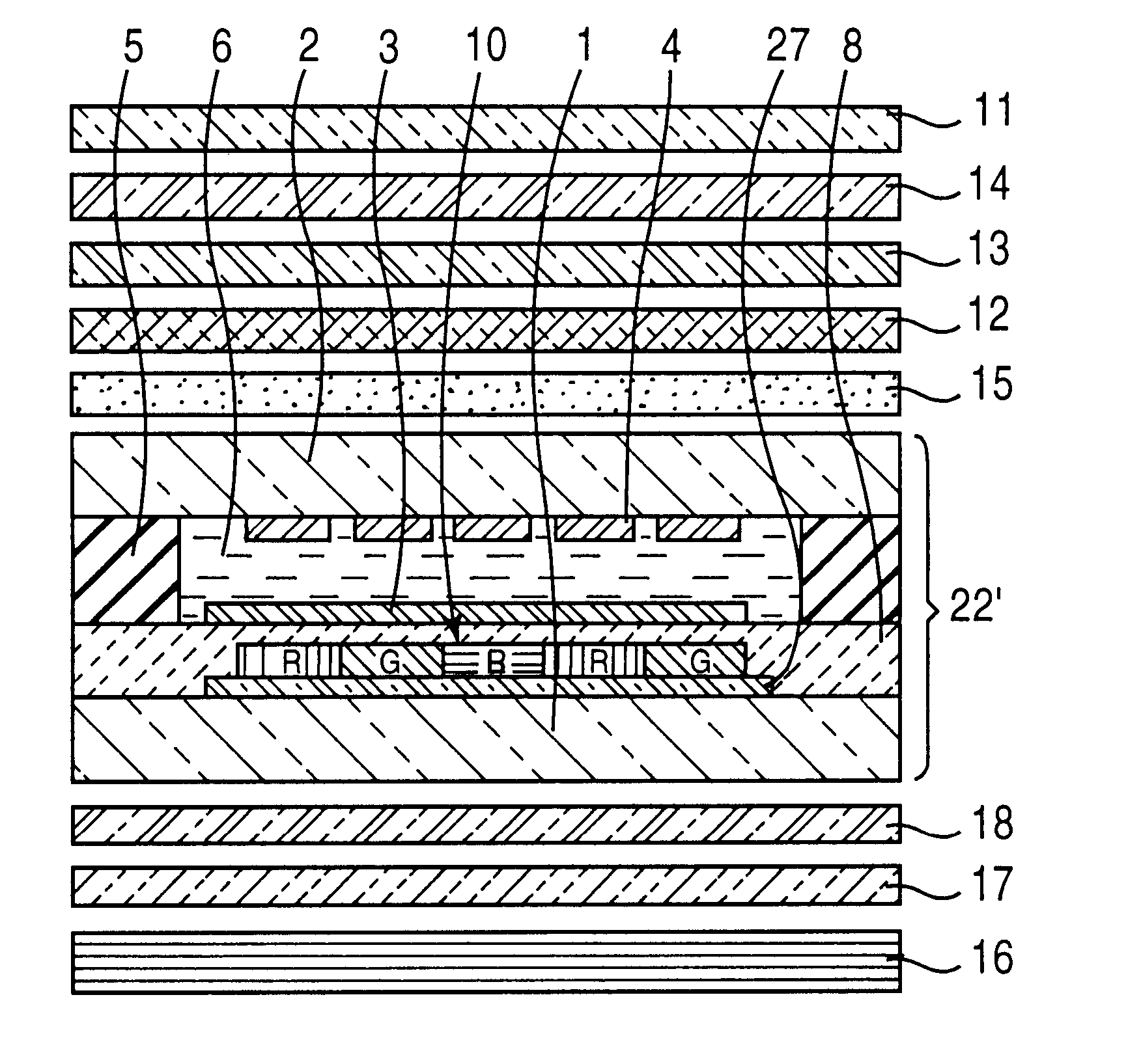
FIG. 9 is a schematic sectional view showing the constitution of the liquid crystal display device, and FIG. 10 is a plan view showing a planar layout relationship among color filters and first as well as second electrodes (shown by phantom lines) of a liquid crystal element. In the figures, parts corresponding to those in FIGS. 1, 6, and 2 are denoted by the like reference numerals.
The liquid crystal display device according to the third embodiment differs in constitution from the first and second embodiments in that the color filters are installed between a reflector 7 and the first electrodes 3 inside the liquid crystal element, thereby composing a reflection-type liquid crystal display device capable of effecting colored display.
With the liquid crystal display device, the liquid crystal element 22 is provided with the 1 .mu.m thick color filters 10 on the reflector 7 made of 0.2 .mu.m thick aluminum provided on the inner face of the first substrate 1 thereof. The color filters 10 are comprised of filters in three colors, red filters R, green filters G, and blue filters B, and are formed in alternate and parallel stripes so as to correspond to the second electrodes 4 patterned in stripes, formed on the inner face of the second substrate 2. The respective color filters R, G, B are formed to have a width wider than that of the respective second electrodes 4 so as not have a gap therebetween. It is not desirable that there exists a gap between the respective color filters 10 because this will cause white light to be mixed with display colors, and degrade color purity although a quantity of incident light is increased and display of images becomes brighter.
The constitution of the liquid crystal element 22, in other respects, is the same as that of the liquid crystal element 20 shown in FIG. 1, and description thereof is therefore omitted.
As with the case of the second embodiment shown in FIG. 6, on the outer side (the visible side) of the second substrate 2 of the liquid crystal element 22, a diffusion film 15, a twisted retardation film 12, a first retardation film 13, a second retardation film 14, and a polarizing film 11 are disposed in sequence. This embodiment is the same as the second embodiment in respect of the constitution of the respective films described above, joining of the respective films with each other by pasting with an adhesive, and use of the light scattering adhesive for the diffusion film 15.
Further, with this embodiment, a layout relationship between lower and upper molecular alignment directions 6a, 6b of nematic liquid crystal 6 of the liquid crystal element 22 and a transmission axis 11a of the polarizing film 11 is the same as that for the first embodiment shown in FIG. 3. Also, a layout relationship between lower and upper molecular alignment directions 12a, 12b of the twisted retardation film 12, and phase delay axes 13a, 14a of the first and second retardation films 13, 14, respectively, is the same as that for the second embodiment shown in FIG. 8. Accordingly, figures showing these and description thereof are omitted.
For improvement of brightness, the color filters 10 preferably have the maximum transmittance at an optical spectrum as high as possible, and the respective color filters preferably have the maximum transmittance of 80% or more, most preferably 90% or more. Further, the minimum transmittance thereof at an optical spectrum need be as high as 20 to 50%.
For the color filters 10, various types such as a pigment dispersion type, a dyeing type, a printing type, a transfer type, a electrodeposition type and so forth can be used, however, a color filter of the pigment dispersion type made by dispersing a pigment in an acrylic or PVA based photosensitive resin is most preferable because of heat resistance at high temperatures and high color purity.
For obtaining the color filters 10 having a high transmittance, the reflector 7 made up of a thin aluminum film was formed on the inner face of the first substrate 1, the surface of the reflector 7 was inactivated by anodizing, subsequently a color resist with 10 to 15% of a pigment blended with photosensitive resin was applied to the inner face of the first substrate 1 by use of a spinner, and a exposure and development treatment was applied thereto, whereupon the 1 .mu.m thick color filters 10 having a high transmittance was obtained.
Herein, the effect of the liquid crystal display device according to the third embodiment is described. As described with reference to the first embodiment, when no voltage is applied between the first electrodes 3 and the second electrodes 4 of the liquid crystal element 22 (the liquid crystal element 20 in the case of the first embodiment), the twisted retardation film 12 and the liquid crystal element 22 are fully compensated, so that birefringent tendency does not occur at all.
The second retardation film 14 and the first retardation film 13 have a total retardation value of 0.14 .mu.m at a wavelength of 0.55 .mu.m, and form a so-called wide-band quarter-wavelength film wherein retardation values in a short wavelength region are smaller than those in a long wavelength region, so that the quotients of retardation values divided by wavelengths can be rendered approximately one quarter over the entire visible light region. Consequently, circularly polarized light can be obtained at all wavelengths in the visible light region, enabling perfect black in display to be effected as with the second embodiment.
In FIG. 9, upon linearly polarized light falling on the liquid crystal display device through the polarizing film 11 from the upper visible side, components of the linearly polarized light at all wavelengths in the visible light region are turned into circularly polarized light after passing through the second retardation film 14 and the first retardation film 13.
Since the twisted retardation film 12 and the liquid crystal element 22 are fully compensated while the first electrodes 3, a protective film 8 and the color filters 10 have no birefringent tendency at all, the circularly polarized light undergoes no change in polarization state, and arrives at the reflector 7 as it is.
The circularly polarized light reflected at the reflector 7 undergoes no change even after passing through the liquid crystal element 22 and the twisted retardation film 12, but when passing through the first retardation film 13 and the second retardation film 14, the circularly polarized light reverts to linearly polarized light with the direction of polarization, rotated through 90.degree., and the linearly polarized light is all absorbed by the polarizing film 11, so that perfect black display can be obtained.
When a predetermined voltage is applied between the first electrodes 3 and the second electrodes 4 of the liquid crystal element 22, liquid crystal molecules of the nematic liquid crystal 6 are caused to rise, and a real .DELTA.nd value of the liquid crystal element 22 decreases. Consequently, the linearly polarized light falling on the liquid crystal display device from the visible side through the polarizing film 11 is turned into circularly polarized light after passing through the second retardation film 14 and the first retardation film 13, but reverts to elliptically polarized light or linearly polarized light as a result of passing through the twisted retardation film 12 and the liquid crystal element 22. The elliptically polarized light or linearly polarized light arrives at the reflector 7, and is reflected thereby. The elliptically polarized light or linearly polarized light as reflected returns without being rotated, and nearly all components thereof are transmitted through the polarizing film 11 to be sent out to the visible side, so that bright white display can be obtained.
By combining a display pixel in the on (white) state with a display pixel in the off (black) state, color display can be effected. For example, red display can be effected by turning a pixel provided with a red filter R "on" (white) and turning pixels provided with a green filter G and a blue filter B, respectively, "off" (black)
With the reflection-type liquid crystal display device according to this embodiment, it was possible to achieve a high reflectance, and a contrast ratio as high as 10 or more, and bright color display having high chroma could be effected.
Thus, by use of the polarizing film 11, the second retardation film 14, the first retardation film 13, the twisted retardation film 12, the diffusion film 15, and the liquid crystal element 22 incorporating the reflector 7 and the color filters 10, installed in this order from the visible side, it becomes possible to obtain display in excellent black and display in bright white, thereby enabling bright display in high contrast to be effected by use of the reflection-type liquid crystal display device of single polarizing film type.
VARIATIONS OF THE THIRD EMBODIMENT
With the third embodiment, an STN liquid crystal element twisted through 240 degrees is used for the liquid crystal element 22, however, even with the use of a TN liquid crystal element having a twist angle of around 90 degrees, a similar reflection-type liquid crystal display device can be obtained.
In the case of effecting display on a large screen by use of the TN liquid crystal element, it is preferable to adopt a liquid crystal display device of an active-matrix mode incorporating active elements such as TFTs, MIMs, and so forth.
With this embodiment, the reflector 7 is formed on the underside of the first electrodes 3 such that the protective film 8 is sandwiched therebetween, however, the first electrodes 3 may be made up of a metal film made of aluminum, silver, and so forth, to be reflective electrodes doubling as the reflector 7. And the color filters 10 may be formed directly on the reflective electrodes.
Further, with this embodiment, the color filters 10 are installed on the side of the first substrate 1, but it may be installed between the second substrate 2 and the second electrodes 4 provided on the side of the second substrate 2, instead.
However, in the case where the color filters 10 are installed on the side of the first substrate 1, the protective film 8 can serve for planarization of the color filters 10, doubling as an insulation film between the reflector 7 and the first electrodes 3.
Furthermore, with this embodiment, for the color filters 10, the filters in three colors of red, green and blue are used, however, with the use of color filters in three colors of cyan, yellow and magenta, similar bright color display can be effected as well.
Still further, with this embodiment, material having the same wavelength dependency of refractive index is used for the first retardation film 13 as well as the second retardation film 14, and both the retardation films are disposed such that the respective phase delay axes cross each other at 60.degree., however, as with the first embodiment, two sheets of the retardation films having different wavelength-dependency of reflective index may be used if disposed such that the respective phase delay axes cross each other at right angles.
PUM


Description & Claims & Application Information
We can also present the details of the Description, Claims and Application information to help users get a comprehensive understanding of the technical details of the patent, such as background art, summary of invention, brief description of drawings, description of embodiments, and other original content. On the other hand, users can also determine the specific scope of protection of the technology through the list of claims; as well as understand the changes in the life cycle of the technology with the presentation of the patent timeline. Login to view more.