Double data rate synchronous memory with block-write
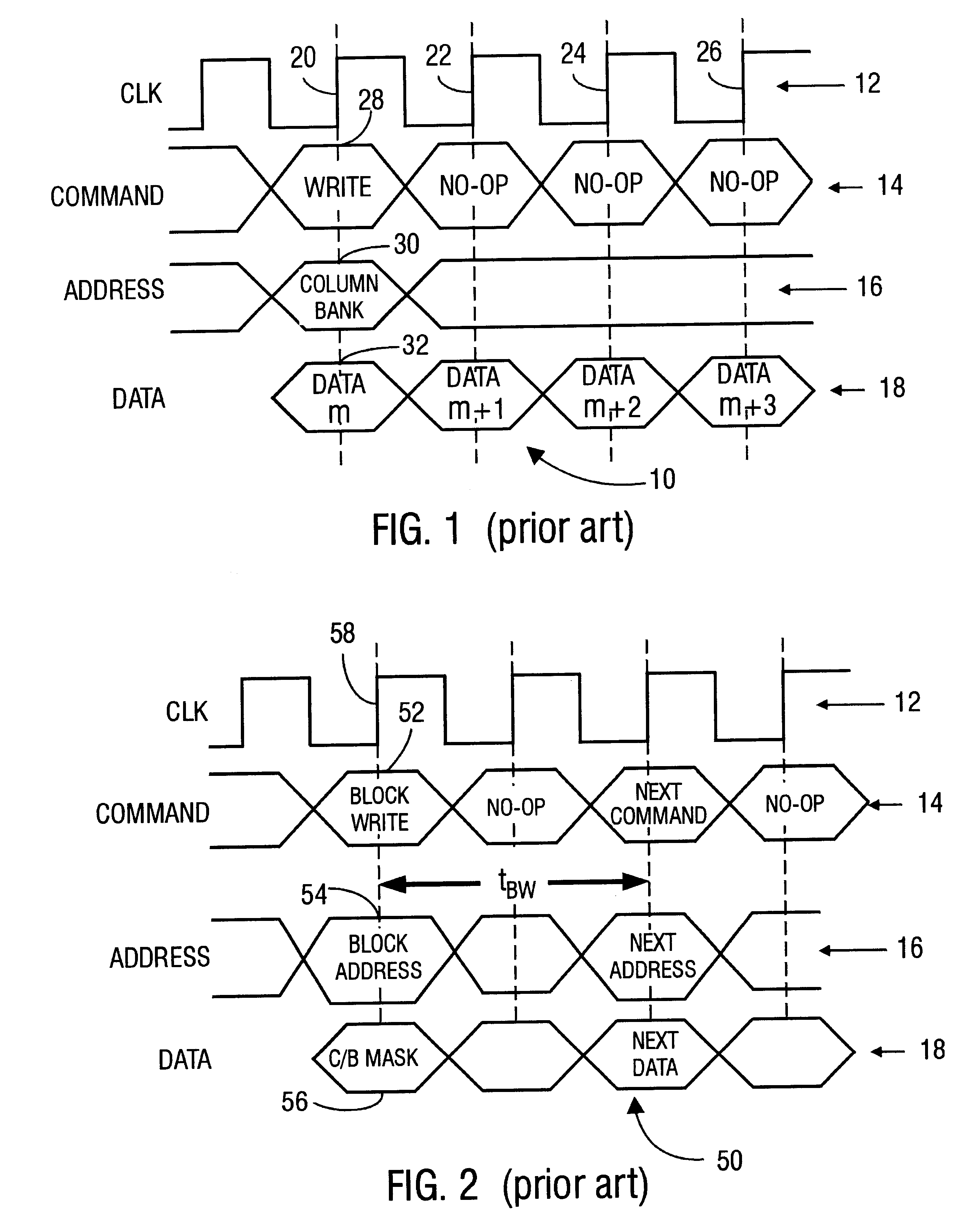
a synchronous memory and data rate technology, applied in the field of double data rate synchronous memory with block-write, can solve the problems of limiting the speed of video applications, enforcing the above-described effective speed of 8-column block-write, and additional cost and complexity of implementing block-writes compared to other alternatives
- Summary
- Abstract
- Description
- Claims
- Application Information
AI Technical Summary
Problems solved by technology
Method used
Image

Examples
first embodiment
FIG. 4 illustrates a memory device 110, which performs block-writes at a double data rate in a manner such as the method 100 of FIG. 3. A data input port 112 receives input data signals having n binary digits from an external bus line carrying n bit data signals (not shown). The data input port 112 connects to even and odd data input latches 114, 116. The even and odd data input latches 114, 116 receive mask data for block-writes. In some embodiments, the data input latches receive both mask data for block-writes and data for ordinary writes to the memory device 110. In some embodiments separate data input latches or registers (not shown) receive the mask data. Then, the number n, equal to the number of input lines and to the number of external bus lines (both not shown) for mask data, is still smaller than the number, 2n, of binary digits of mask data per block-write. The n output lines 118, 120 from each data input latch 114, 116 connect to a block-write mask register 122. The blo...
second embodiment
FIG. 5 illustrates a second embodiment for a memory device 140, which performs block-writes at a double data rate. The data input port 112 couples to even and odd data input latches 114, 116. The even and odd data input latches 114, 116 receive and transmit even and odd portions of the mask data for block writes and even and odd data for normal writes. Output lines 119, 121 individually connect outputs of the even and odd data latches 114, 116 to a write I / O logic unit 142. The memory device 140 includes a block-write data register 128A and multiplexers 128B, 128C, similar to the embodiment of FIG. 4, or alternatively, even and odd block-write data registers 145, 147B, which couple to the write I / O logic unit 142A and 142B by individual output lines 148, 150. The write I / O logic units 142A and 142B transmit the even and odd block-write data to separate even and odd memory locations 131, 133 of the memory bank 132. In the memory device 140, the internal lines 119, 121, for block-writ...
embodiment 180
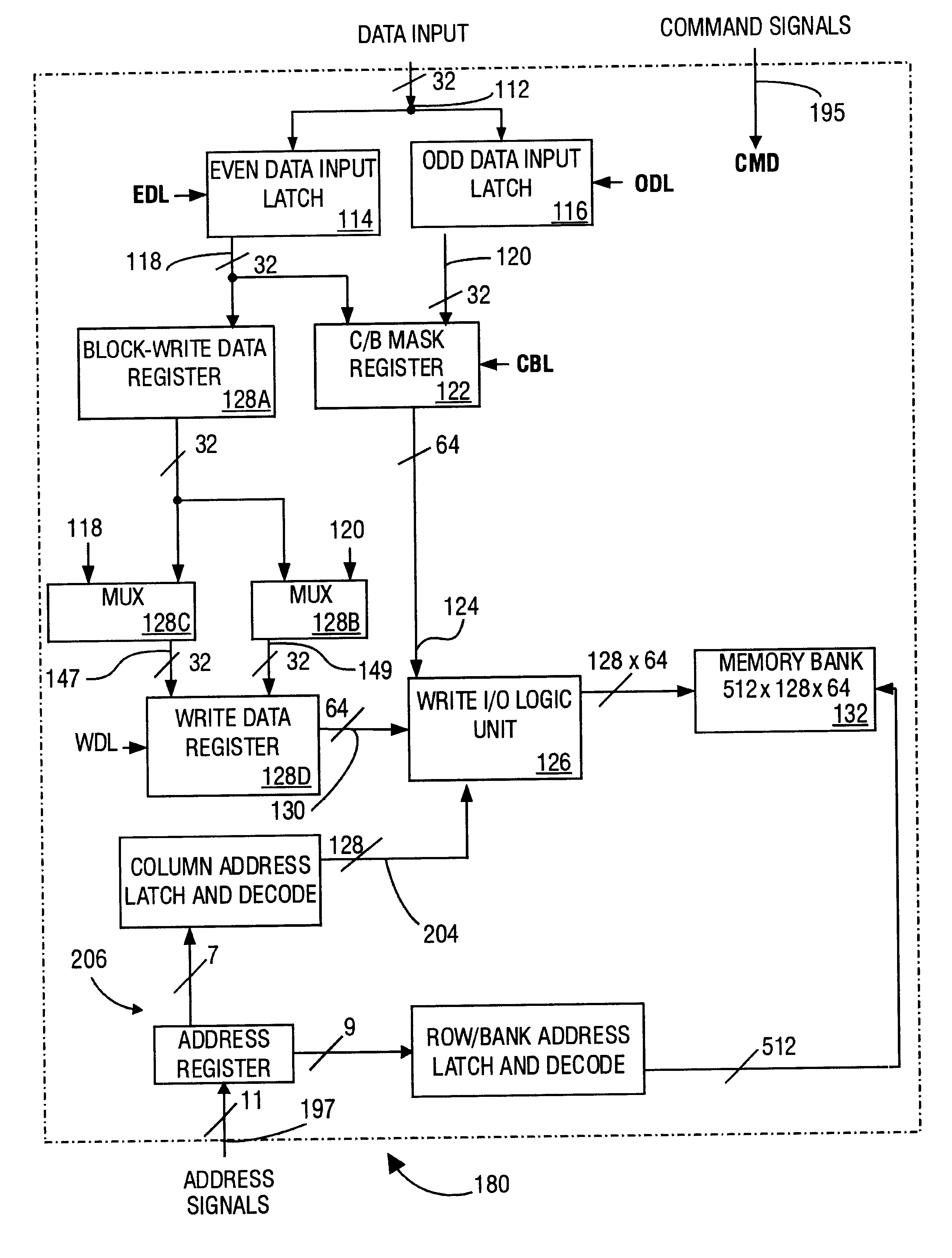
FIG. 10 illustrates a specific embodiment 180 of the memory device 110 of FIG. 4. The data input port 112 connects, in parallel to the even and odd data input latches 114, 116. The even and odd data input latches 114, 116 transfer even and odd write data, block-write data, and even and odd column / byte (C / B) mask data from the data input port 112 to the respective register, over signal lines 118 and 120, in response to appropriate command signals described below. Since input data signals have 32 binary digits and the internal column / byte (C / B) mask data 124 and write / block-write data signals 130 have 64 binary digits, the memory device 180 performs all write operations at a double data rate.
Still referring to FIG. 10, write I / O logic unit 126 receives write / block-write data, mask data and column select control from the lines 130, 124, and 204, respectively. The write I / O logic unit 126 controls both writes and block-writes. Address logic 206 enables row addresses of the memory bank 1...
PUM
 Abstract
Description
Claims
Application Information
 - R&D
- Intellectual Property
- Life Sciences
- Materials
- Tech Scout
- Unparalleled Data Quality
- Higher Quality Content
- 60% Fewer Hallucinations
Browse by: Latest US Patents, China's latest patents, Technical Efficacy Thesaurus, Application Domain, Technology Topic, Popular Technical Reports.
© 2025 PatSnap. All rights reserved.Legal|Privacy policy|Modern Slavery Act Transparency Statement|Sitemap|About US| Contact US: help@patsnap.com