Magnetic and electric shielding of on-board devices

a technology of magnetic and electric shielding, which is applied in the direction of semiconductor devices, semiconductor/solid-state device details, electrical apparatus casings/cabinets/drawers, etc., can solve the problems of assisting a given system in achieving compliance with the fcc open box regulations

Inactive Publication Date: 2003-05-20
INTEL CORP
View PDF9 Cites 136 Cited by
  • Summary
  • Abstract
  • Description
  • Claims
  • Application Information

AI Technical Summary

Problems solved by technology

However, the primary layer 20 offers no magnetic shielding or electric shielding for the device 12 for emitted (or r

Method used


Image

  • Magnetic and electric shielding of on-board devices
  • Magnetic and electric shielding of on-board devices
  • Magnetic and electric shielding of on-board devices

Examples


first embodiment

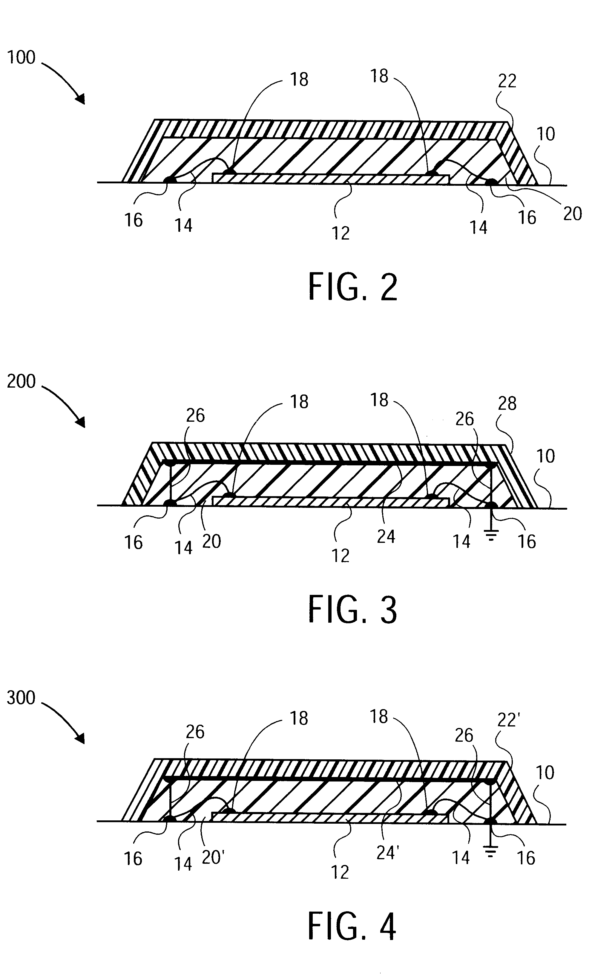
Reference is now made to FIG. 2, which shows a system 100 encapsulating the device 12 on the surface 10 of a device board (i.e., the device 12 may be an on-board device) in accordance with a first embodiment of the invention. The system 100 is somewhat similar to the system 50 except for the provision of a "tertiary" layer 22 that encapsulates or covers completely, or covers a portion of (e.g., a substantial portion of), the primary layer 20 (the layer 22 is termed "tertiary" for reasons set forth below). Covering only a portion may be due to, for example, air bubbles, imperfections, or it may be done by design. However, for shielding purposes, complete or substantial covering, as understood by those skilled in the art in the context of the present invention, may be desirable to maximize shielding. (This discussion of covering applies to all embodiments of the present invention, and for any type of covering layer, not just those of the first embodiment.) The tertiary layer 22 may be...

second embodiment

Referring now to FIG. 3, a system 200 is shown in accordance with a second embodiment of the invention. The system 200 is somewhat similar to the system 100, but the system 200 does not include the tertiary layer 22. Instead, the system 200 includes a "secondary" layer 24 that is electrically conductive, and may be highly conductive. The secondary layer 24 is adjacent or layered on the primary layer 20 encapsulant, and may completely cover, or cover only a portion of, the layer 20. The secondary layer 24 also includes conductive shielding contacts or sections 26 coupled to the contact 16 which, in turn, are coupled to a device board ground (not shown in specific detail). The device contact 18 may also be coupled via the bond wire 14 to the device board ground. An encapsulant layer 28 is included that is adjacent or layered on (and covers all of, or a portion of, e.g., a substantial portion of) the secondary layer 24 and the primary layer 20, such that the secondary layer is disposed...

third embodiment

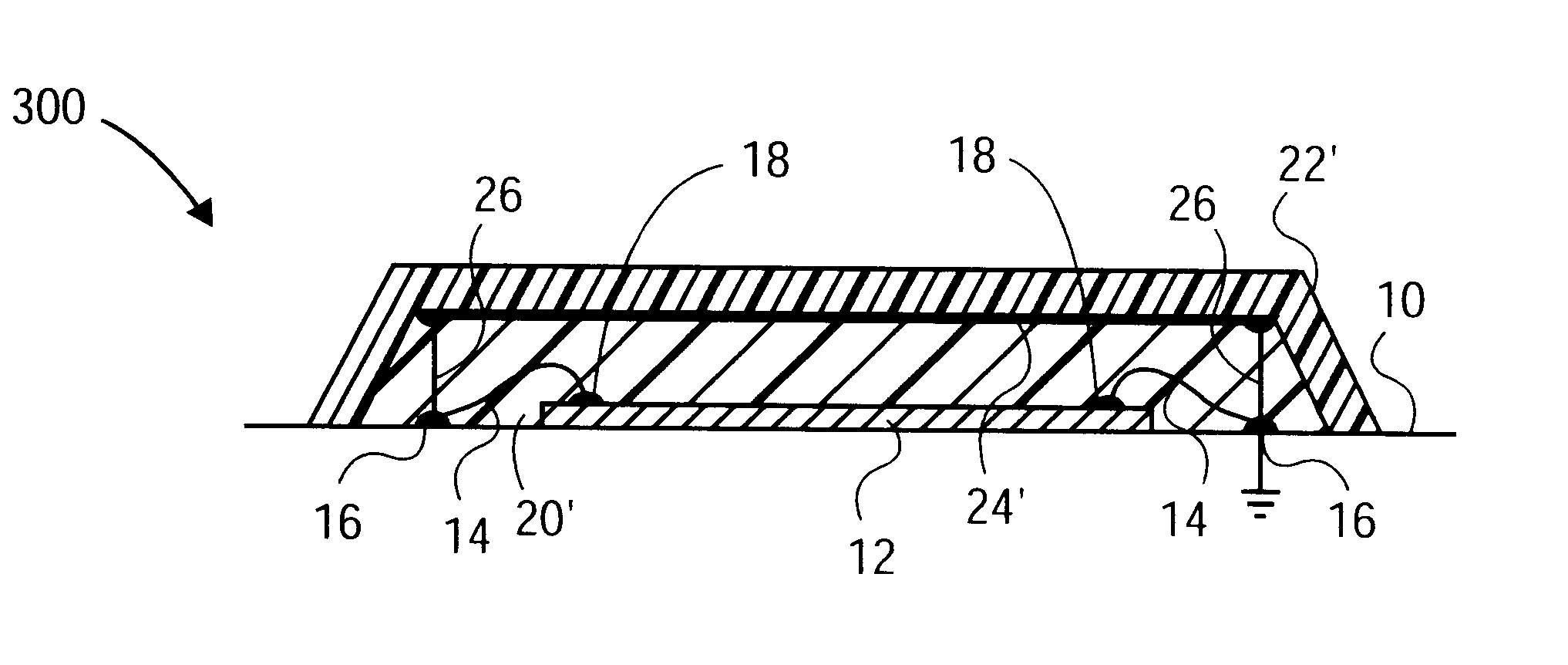
Referring now to FIG. 4, a system 300 is shown in accordance with a third embodiment of the invention. The system 300 incorporates all the functionality of, and similar features to, both the systems 100 and 200 shown in FIGS. 1 and 2. The system 300 includes a primary layer 20' (similar to the primary layer 20), a secondary layer 24' (similar to the secondary layer 24), and a tertiary layer 22' (similar to the tertiary layer 22). The secondary layer 24' is adjacent or layered on (completely covering, or covering a portion of, e.g., a substantial portion of) the primary layer 20', analogous to the layering of the secondary layer 24 on the primary layer 20 in the system 200. Moreover, the tertiary layer 22' is adjacent or layered on (completely covering, or covering a portion of, e.g., a substantial portion of) the secondary layer 24', such that the secondary layer is disposed between the tertiary layer 22' and the primary layer 20', analogous to the layering of the encapsulant layer ...


PUM


Abstract

Improved electromagnetic compatibility for integrated motherboard or device board designs is provided by magnetic shielding, electric shielding, or both integrated into the chip packaging materials. Motherboard emissions may be reduced by use of the shielding. A nonconductive primary and tertiary layer sandwich a high-conductivity metal secondary layer forming a Faraday cage for electric field shielding. A nonconductive primary layer is covered by a tertiary layer formed of a composite having permeable material for magnetic shielding. The tertiary layer formed of a composite could include a high permeability particulate ferrous material. Both the secondary layer and the tertiary layer formed of a composite could be used for both electric and magnetic shielding of chips.

Description

1. Field of the InventionThe invention relates to packaging of circuit board devices, and, in particular, to circuit board device magnetic and electric field shielding.2. Description of Related ArtMotherboard designers today are faced with tighter electromagnetic compatibility ("EMC") regulations than previously. The Federal Communications Commission ("FCC") recently imposed the so-called "open box" electromagnetic interference ("EMI") testing criteria. The open box criteria transfers responsibility for regulation of computer system (i.e., unintentional radiator's) radiated energy produced by on-board components, such as application specific integrated circuits ("ASICs"), from a shielded enclosure (e.g., a computer case or enclosure) housing the components to the internal components themselves, specifically a motherboard. Such emissions, which previously could be sufficiently attenuated by the shielded enclosure to satisfy the prior "closed box" regulations, must now be sufficiently...

Claims


Application Information

Patent Timeline
IPC IPC(8): H01L23/552H01L23/28H01L23/31H05K9/00
CPCH01L23/3135H01L23/552H01L24/48H01L24/49H01L2924/10253H01L2924/00014H01L2924/3025H01L2924/19107H01L2924/16152H01L2924/1433H01L2924/14H01L2924/01079H01L2924/0103H01L2924/01029H01L2924/01028H01L2924/01025H01L2224/05599H01L2224/48091H01L2224/48465H01L2224/4911H01L2224/85399H01L2924/01013H01L2924/01014H01L2224/45099H01L2924/00H01L2924/12032H01L2924/181H01L2924/00012
Inventor ASKEW, RAY
Owner INTEL CORP
Why Eureka
Try Eureka