
Method and apparatus for dynamic model building based on machine disturbances for run-to-run control of semiconductor devices

a dynamic model and model building technology, applied in the field of semiconductor product manufacturing, can solve the problems of only updating a few of the settings of the exposure tool, and changing the effectiveness of control settings

Inactive Publication Date: 2003-06-10
ADVANCED MICRO DEVICES INC
View PDF12 Cites 22 Cited by
  • Summary
  • Abstract
  • Description
  • Claims
  • Application Information

AI Technical Summary

Problems solved by technology

Among the factors that affect semiconductor processing are machine disturbances.
Machine disturbances include external factors such as temperature, humidity, and idle time between processes.
Some of the problems associated with the current methods include the fact that the exposure tool settings are only updated a few times a month.
Machine disturbances can also change the effectiveness of control settings.

Method used


Image

  • Method and apparatus for dynamic model building based on machine disturbances for run-to-run control of semiconductor devices
  • Method and apparatus for dynamic model building based on machine disturbances for run-to-run control of semiconductor devices
  • Method and apparatus for dynamic model building based on machine disturbances for run-to-run control of semiconductor devices

Examples


Embodiment Construction

Illustrative embodiments of the invention are described below. In the interest of clarity, not all features of an actual implementation are described in this specification. It will, of course, be appreciated that in the development of any such actual embodiment, numerous implementation-specific decisions must be made to achieve the developers' specific goals, such as compliance with system-related and business-related constraints, which will vary from one implementation to another. Moreover, it will be appreciated that such a development effort might be complex and time-consuming, but would nevertheless be a routine undertaking for those of ordinary skill in the art having the benefit of this disclosure.

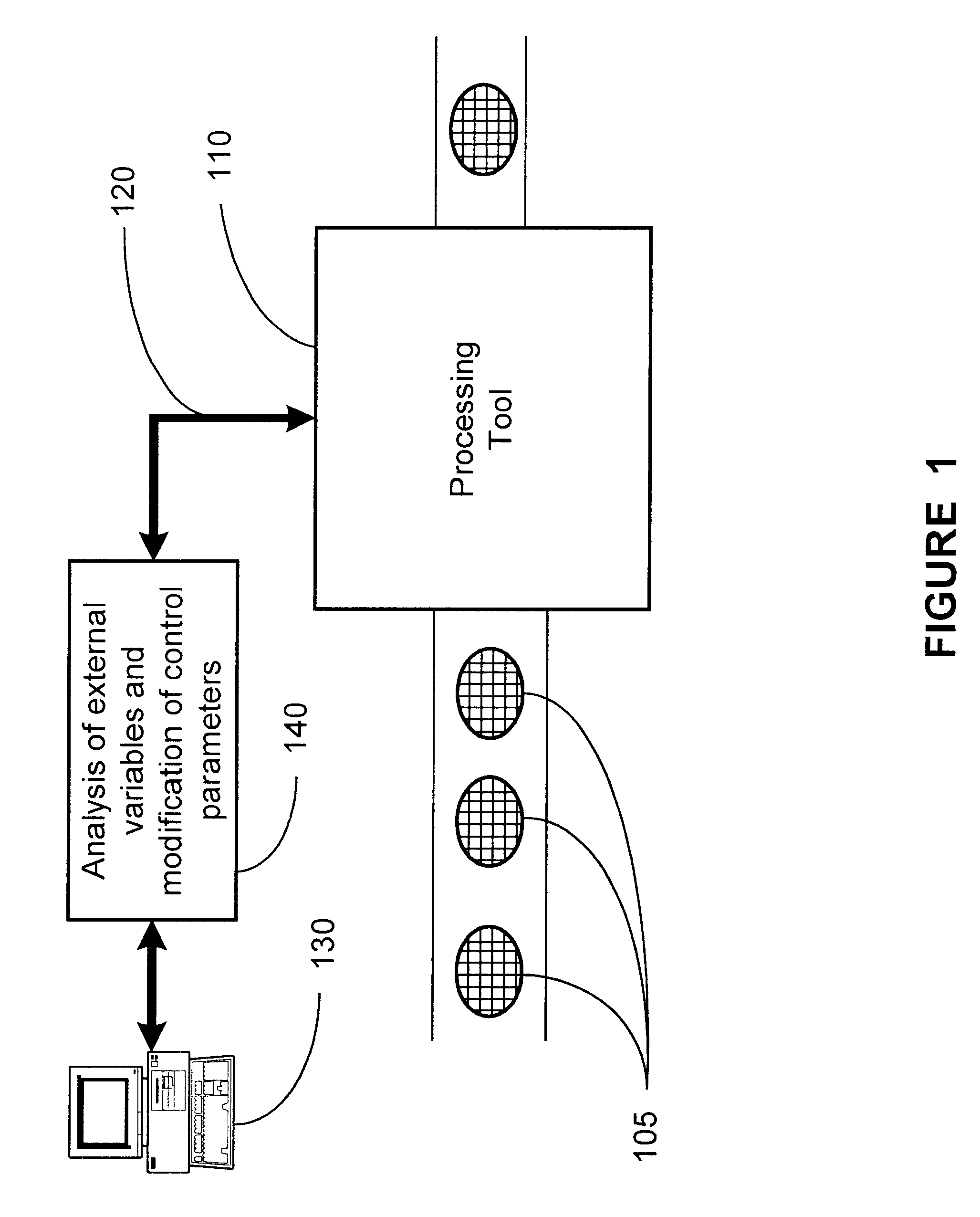
There are many discrete processes that are involved in semiconductor manufacturing. Many times, semiconductor devices are stepped through multiple manufacturing process tools. External variables, such as temperature, pressure, and delays between processes, can cause unanticipated var...


PUM


Abstract

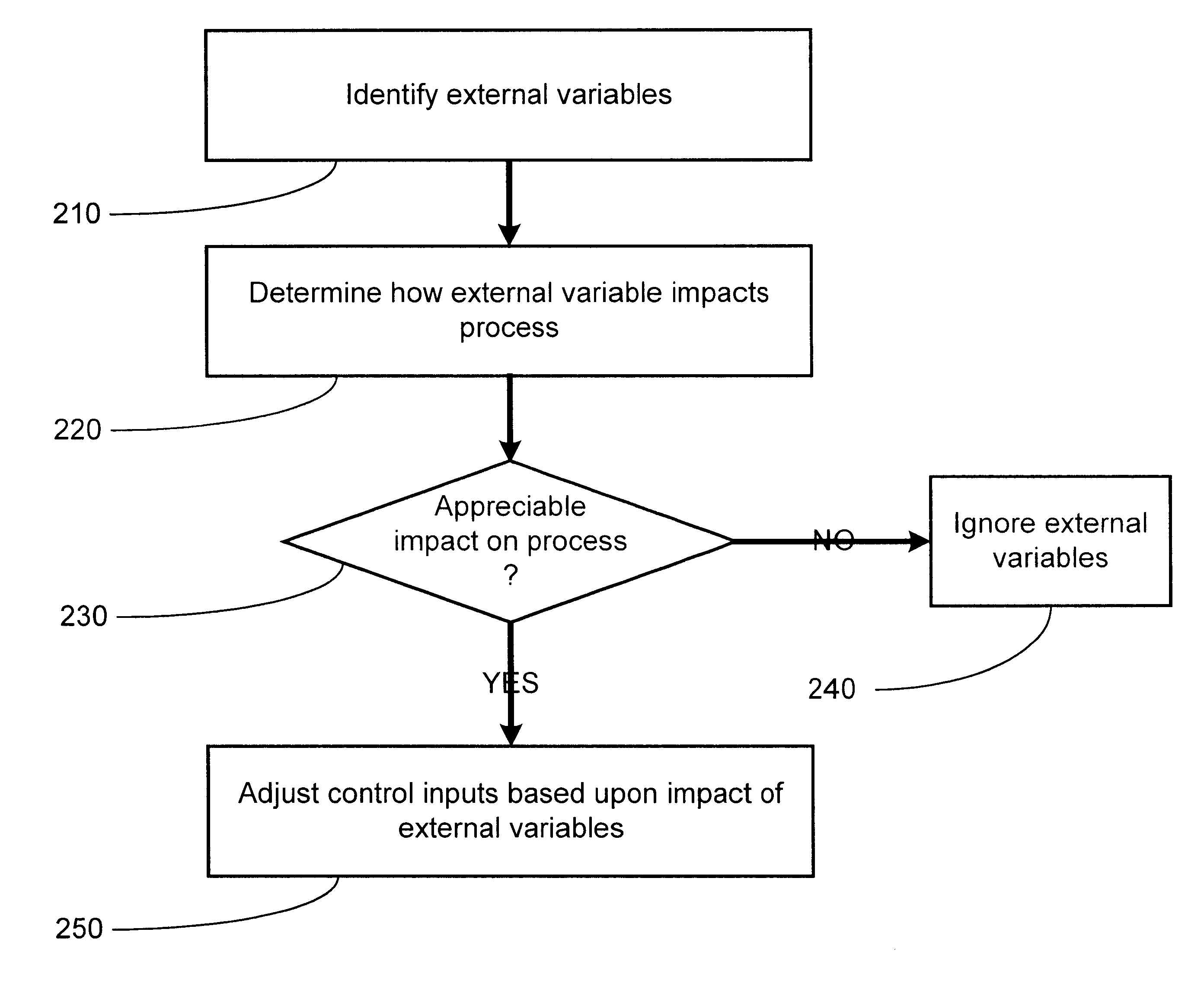
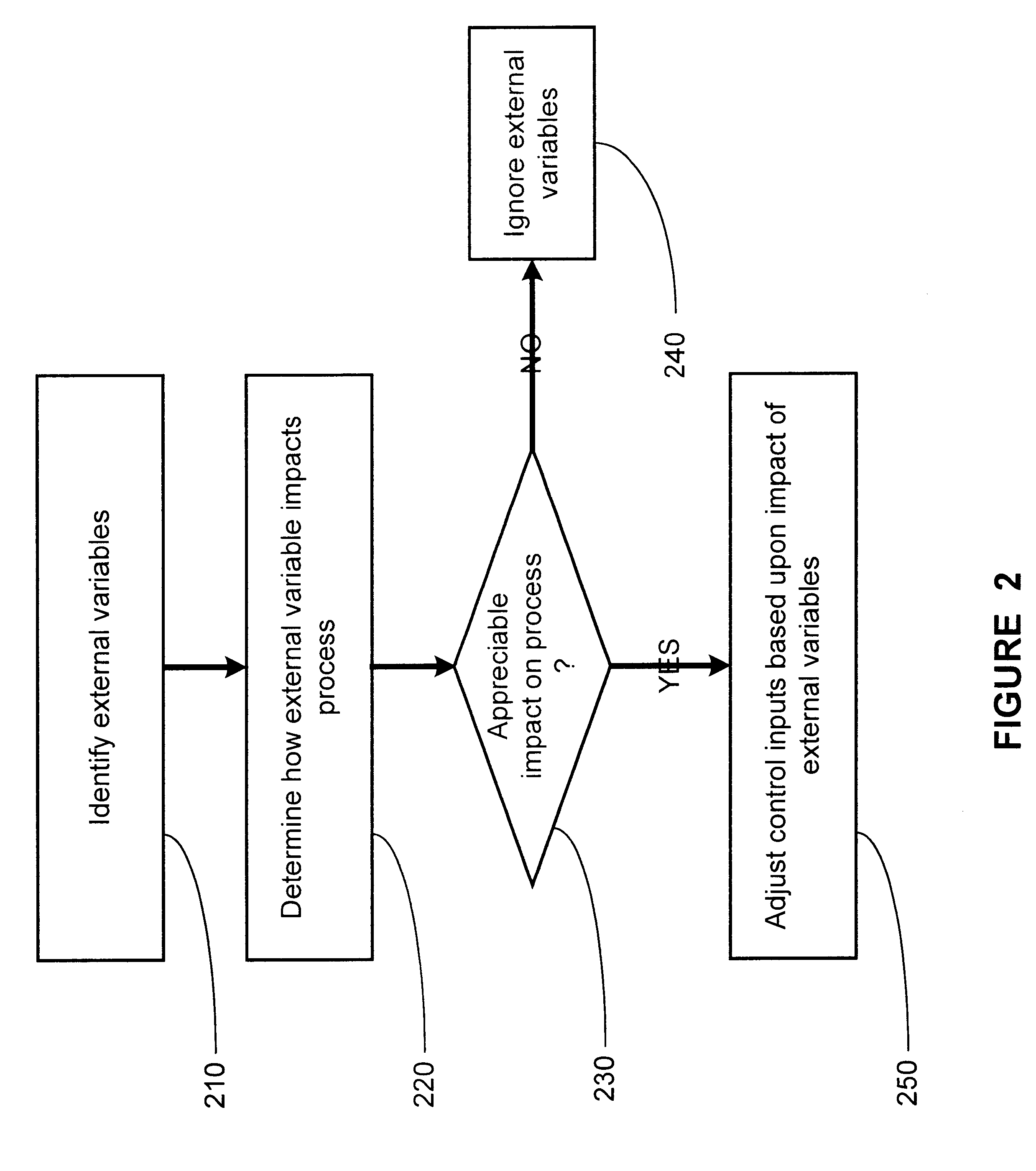
The present invention provides a method and apparatus for correction of machine disturbances for run-to-run control of semiconductor device manufacturing processes. At least one external variable is identified. How the external variable impacts a semiconductor device manufacturing process is determined. A determination whether the impact of the external variable causes an appreciable impact on the semiconductor device manufacturing process is made. At least one control parameter of the semiconductor device manufacturing process is adjusted in response to the determination that the impact of the external variable causes an appreciable impact on the semiconductor device manufacturing process.

Description

1. Field of the InventionThis invention relates generally to semiconductor products manufacturing, and, more particularly, to a method and apparatus for compensation of process control in response to machine disturbances for run-to-run control of semiconductor manufacturing processes.2. Description of the Related ArtThe technology explosion in the manufacturing industry has resulted in many new and innovative manufacturing processes. Today's manufacturing processes, particularly semiconductor manufacturing processes, call for a large number of important steps. These process steps are usually vital, and, therefore, require a number of inputs that are generally fine-tuned to maintain proper manufacturing control.The manufacture of semiconductor devices requires a number of discrete process steps to create a packaged semiconductor device from raw semiconductor material. The various processes, from the initial growth of the semiconductor material, the slicing of the semiconductor crysta...

Claims


Application Information

Patent Timeline
Patent Type & Authority Patents(United States)
IPC IPC(8): G05B5/00G05B5/01G05B19/418
CPCG05B5/01G05B19/41865G05B2219/45031G05B2219/32058Y02P90/02
Inventor BODE, CHRISTOPHER A.
Owner ADVANCED MICRO DEVICES INC
Learn More