Method of forming a raised contact for a substrate

Inactive Publication Date: 2003-07-22
INTEL CORP
View PDF4 Cites 81 Cited by
  • Summary
  • Abstract
  • Description
  • Claims
  • Application Information

AI Technical Summary

Problems solved by technology

In the past, issues of scaling have generally involved either the transistor in the front-end of semiconductor processing or the wiring in the back-end of semiconductor processing.

Method used


Image

  • Method of forming a raised contact for a substrate
  • Method of forming a raised contact for a substrate
  • Method of forming a raised contact for a substrate

Examples


Embodiment Construction

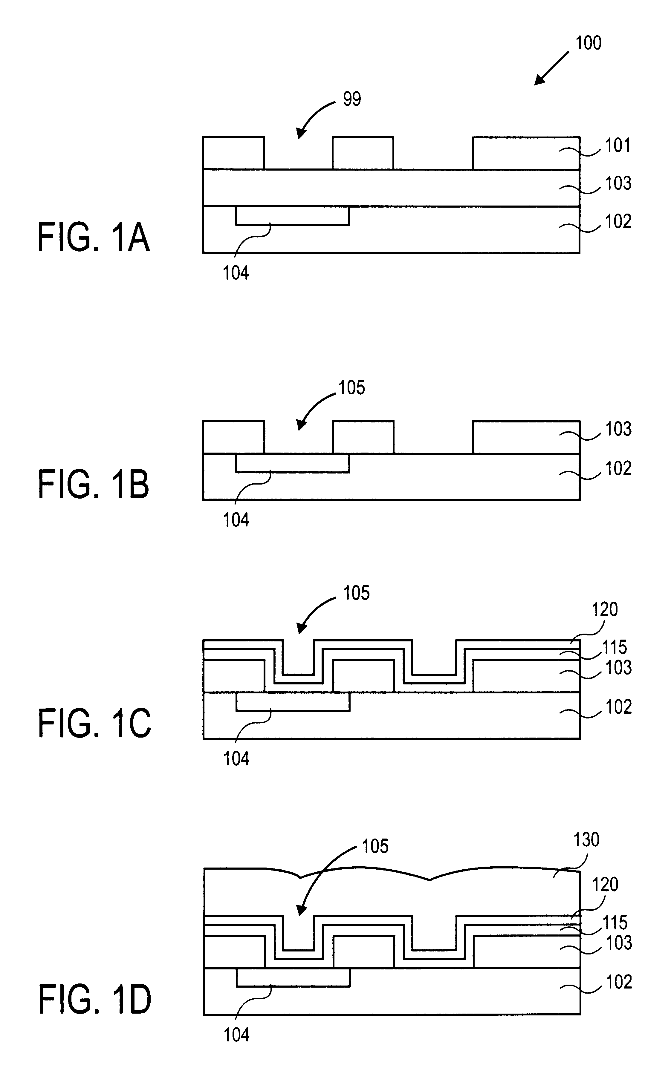
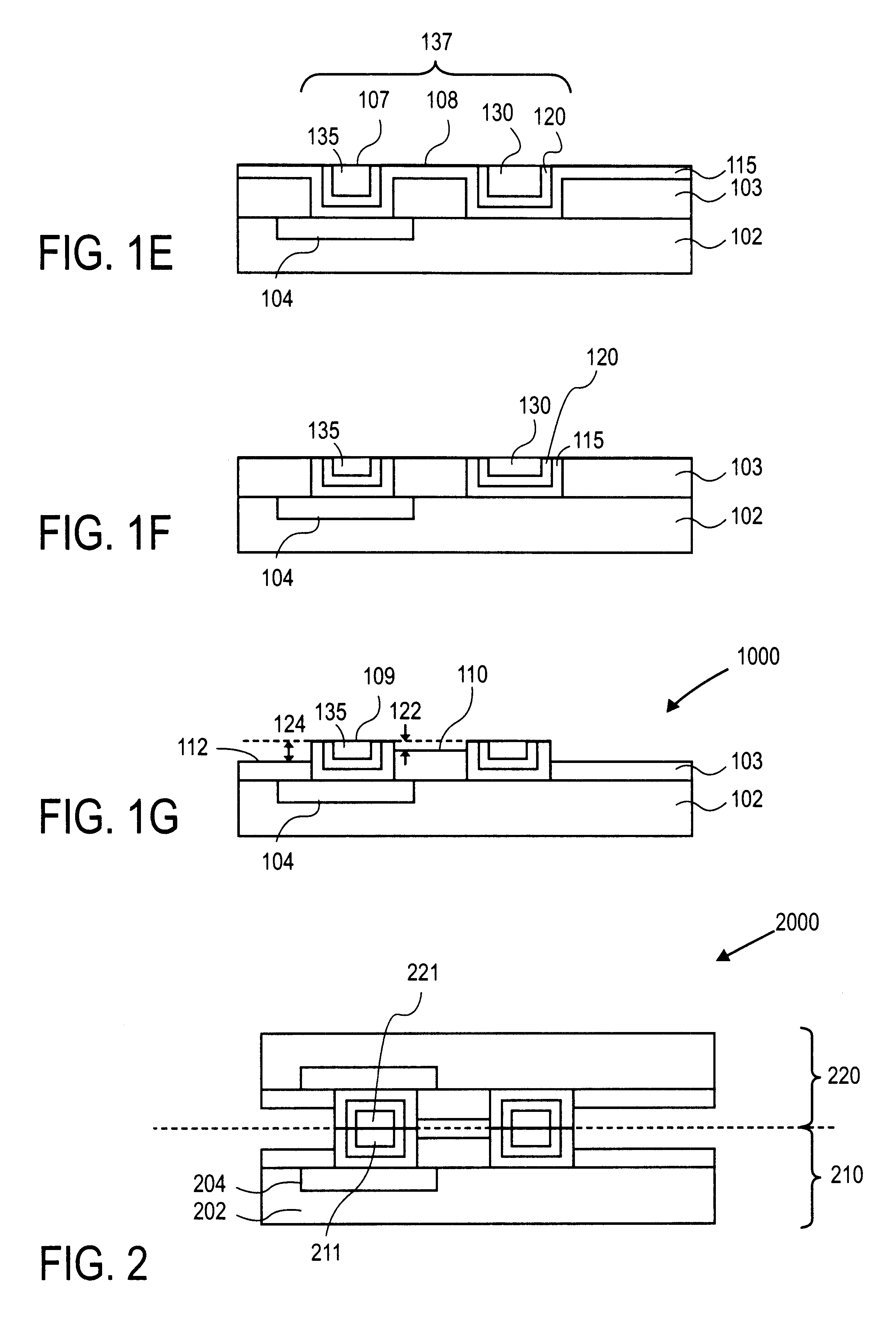
In the following description, numerous details, such as specific materials, dimensions, and processes, are set forth in order to provide a thorough understanding of the present invention. However, one skilled in the art will realize that the invention may be practiced without these particular details. In other instances, well-known semiconductor equipment and processes have not been described in particular detail so as to avoid obscuring the present invention.

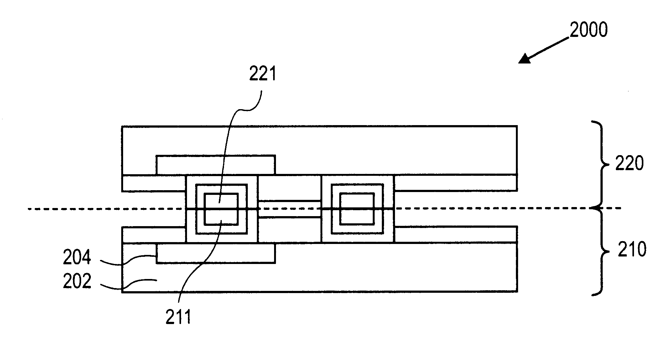
A device may be formed on a substrate by iteratively performing some combination of unit processes such as doping, depositing, patterning, and etching. During the fabrication of integrated circuits (ICs) on a chip or substrate, transistors may be formed in semiconductor material and separated by an electrically insulating material. The transistors may then be wired up with an interconnect system that has multiple layers of an electrically conductive material separated by the electrically insulating material.

A higher device dens...


PUM


Abstract

The present invention includes a method of providing a first substrate; forming an insulator over the first substrate; forming an opening in the insulator; forming a conductor over the insulator and in the opening; removing the conductor over the insulator with a first chemical-mechanical polish process to leave the conductor in the opening; and reducing thickness of the insulator with a second chemical-mechanical process to permit the conductor in the opening to protrude.The present invention further includes a structure having such a conductor that protrudes.

Description

1. Field of the InventionThe present invention relates to the field of semiconductor integrated circuit (IC) manufacturing, and more specifically, to a method of forming raised contacts for a substrate.2. Discussion of Related ArtIn 1965, Gordon Moore first observed that the number of transistors per unit area on a chip appeared to double approximately every 18 months. Ever since then, the semiconductor industry has managed to introduce new designs and processes on schedule to deliver the improvement in device density projected by the so-called Moore's Law. In particular, major enhancements in optics and photolithography have reduced the critical dimension (CD) that can be successfully patterned in the features on a chip or other substrate. At the same time, significant improvements in doping, deposition, and etch have decreased the concentration, depth, and thickness that can be precisely achieved across the substrate.As device dimensions approach atomic dimensions, the fundamental...

Claims


Application Information

Patent Timeline
Patent Type & Authority Patents(United States)
IPC IPC(8): H01L21/00H01L21/70H01L23/48H01L21/302H01L23/485H01L21/02H01L21/768H01L25/065H01L21/321H01L21/60H01L23/522H01L23/532
CPCH01L21/3212H01L24/80H01L24/11H01L24/16H01L25/0657H01L24/13H01L21/7684H01L23/5222H01L2224/05572H01L2224/80895H01L2224/0401H01L2924/0001H01L23/5329H01L24/81H01L2224/05546H01L2224/1147H01L2224/13099H01L2224/81193H01L2224/81801H01L2225/06513H01L2924/01013H01L2924/01016H01L2924/01022H01L2924/01027H01L2924/01029H01L2924/01033H01L2924/01058H01L2924/01073H01L2924/01074H01L2924/01078H01L2924/01082H01L2924/04941H01L2924/04953H01L2924/14H01L2924/19043H01L2924/30105H01L2924/01005H01L2924/01006H01L2924/01019H01L2924/0002H01L2924/12H01L2224/05552H01L24/05H01L2224/05124H01L2224/05147H01L2224/05166H01L2224/05181H01L2224/05184H01L2224/05547H01L2224/05647H01L2924/00014H01L2924/013
Inventor FISHCER, PAUL B.BOARDMAN, JAMES A.MILLER, ANNE E.
Owner INTEL CORP
Why Eureka
Try Eureka