Shielded case, electronic device having shielded case, electronic apparatus using electronic device, and method for manufacturing shielded case

a shielded case and electronic device technology, applied in the direction of casing/cabinet/drawer details, support structure mounting, rack/frame construction, etc., can solve the problems of sensor subject, risk of separation, and threat to the integrity of the shielded cas

Inactive Publication Date: 2003-09-30
MURATA MFG CO LTD
View PDF7 Cites 7 Cited by
  • Summary
  • Abstract
  • Description
  • Claims
  • Application Information

AI Technical Summary

Benefits of technology

It is another object of the present invention to provide a shielded case in which mating parts are not likely to separate from each other and in which gaps between the mating parts can be reduced without the use of solder.
In the shielded case according to the present invention, the half walls are coupled with each other without gaps therebetween, whereby electromagnetic waves inside can be prevented from leaking to the outside and the outside electronic waves can be reliably shielded.
In the electronic device according to the present invention, half walls of a shielded case are firmly coupled with each other, whereby a risk in that the sidewalls remove from each other and an electronic element received in the shielded case is exposed to the outside when an impact is applied is avoided.
In the electronic apparatus according to the present invention, an electronic device is used, in which a risk that the half walls of a shielded case will separate from each other and expose an electronic element received in the shielded case to external electromagnetic radiation when an impact is applied to the case is avoided.

Problems solved by technology

Such sensors are subject to strong impacts which threaten the integrity of the shielded case.
Because these mating parts only interlock with one another, there is a risk that they will separate when an external impact is applied to the shielded case.
If this happens, a gap will be formed between the mating parts and the electronic element in the case will not be sufficiently shielded from electromagnetic waves.
However, this requires an additional manufacturing step and creates a problem of environmental pollution because of the lead in the solder.

Method used


Image

  • Shielded case, electronic device having shielded case, electronic apparatus using electronic device, and method for manufacturing shielded case
  • Shielded case, electronic device having shielded case, electronic apparatus using electronic device, and method for manufacturing shielded case
  • Shielded case, electronic device having shielded case, electronic apparatus using electronic device, and method for manufacturing shielded case

Examples


first embodiment

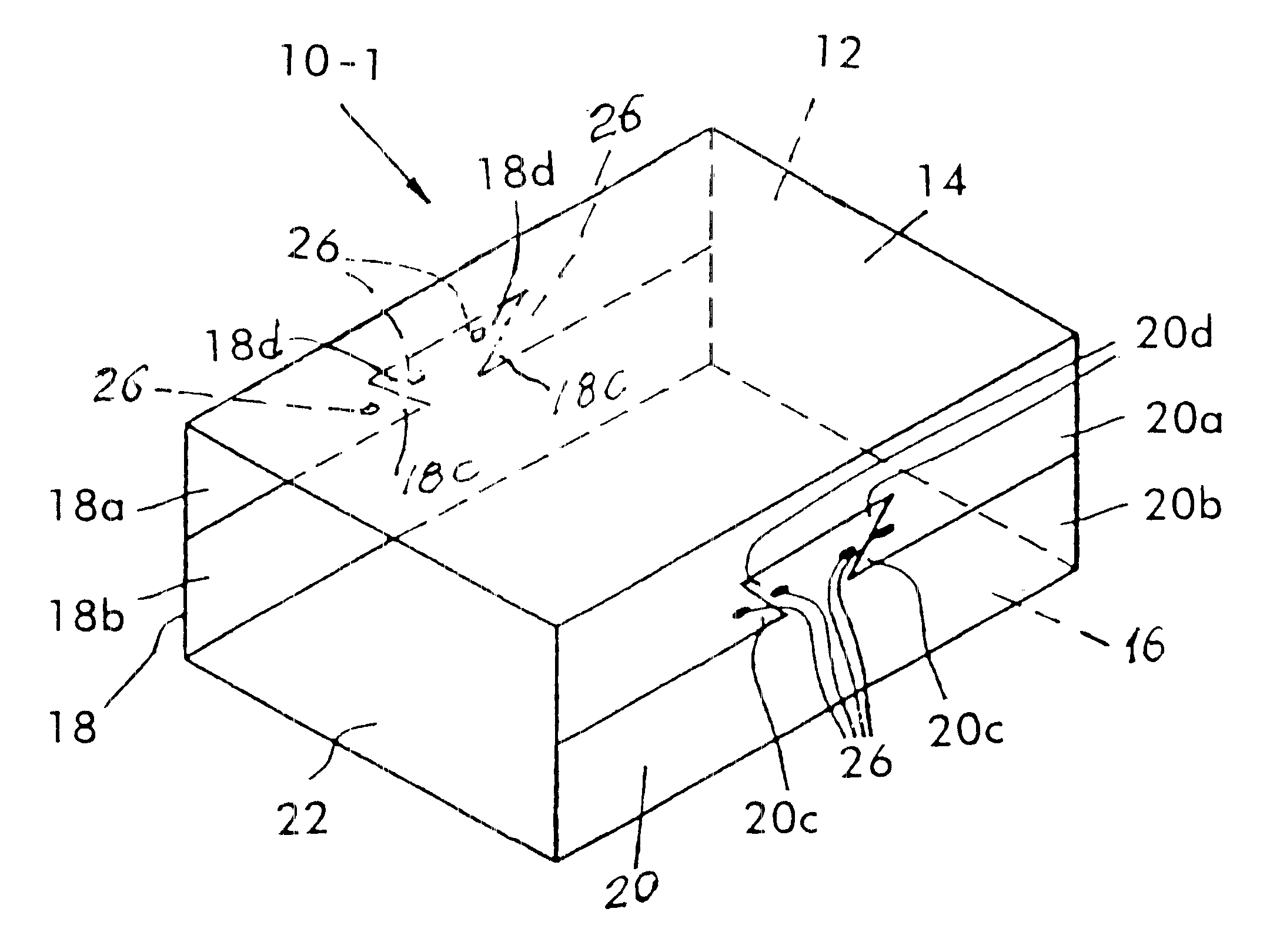
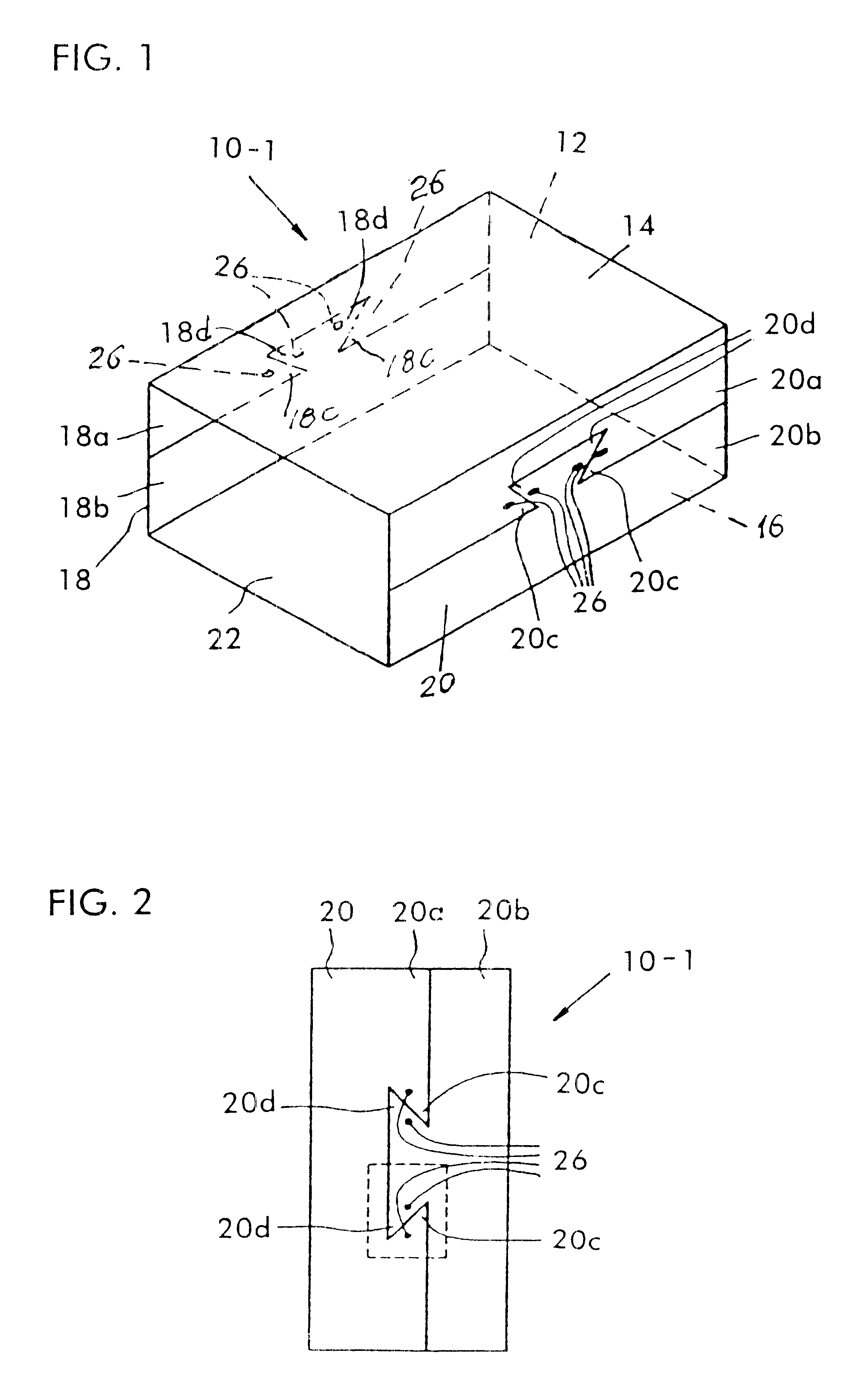
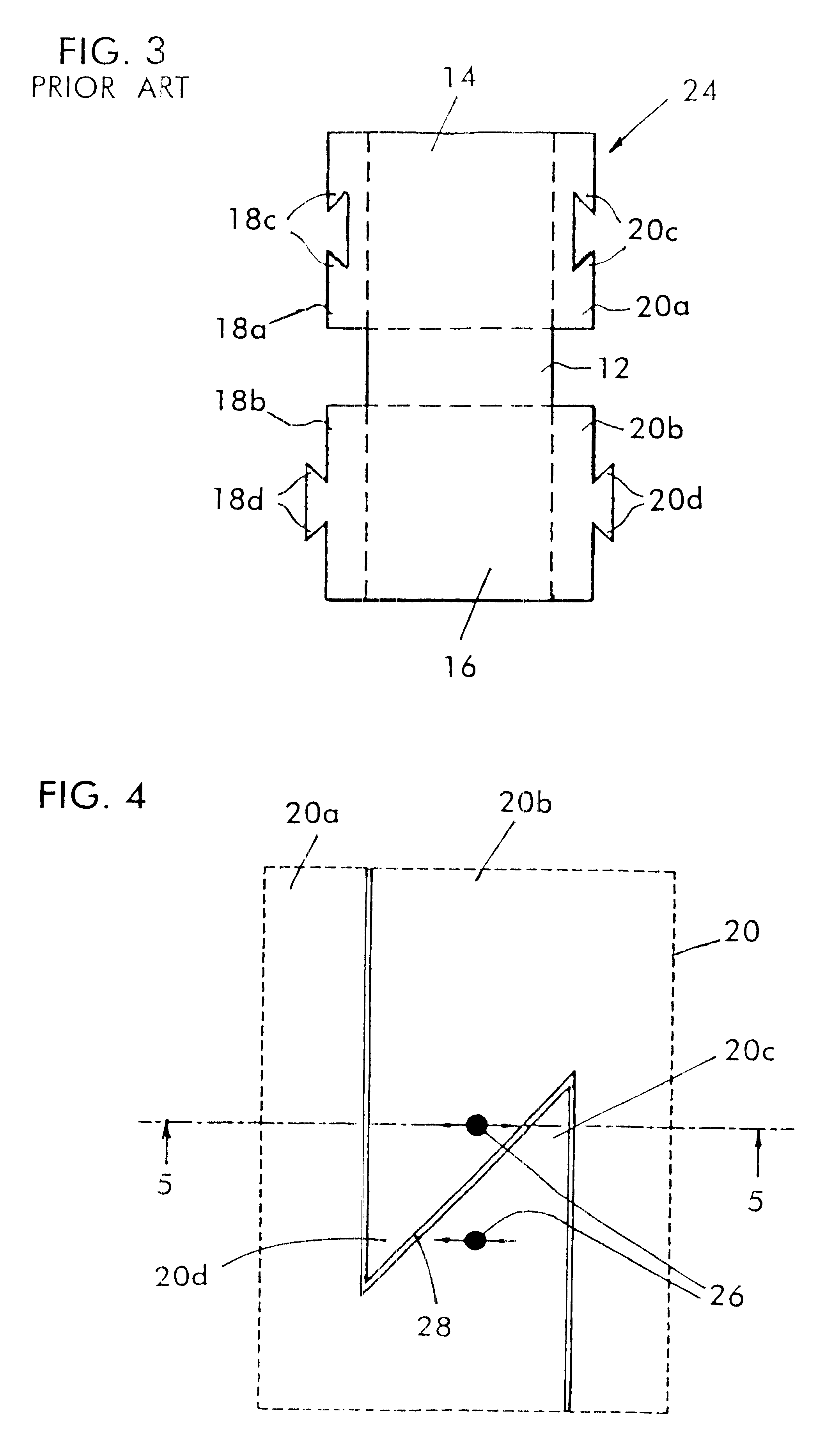
A first embodiment of the present invention is shown in FIGS. 1 through 5. Like the prior art shielded case 10, the shielded case 10-1 of the invention includes a top wall 12, a front wall 14, a rear wall 16 and a pair of side walls 18, 20. The basic structure of the present invention is substantially the same as the prior art and will not be described again. The primary difference between the prior art and the first embodiment of the invention is that the blank 24 is made of a ductile material which is expanded in the area of mating parts 18c, 18d, 20c and 20c by a series of deformations formed in the ductile material in the area of the mating parts. In the embodiment shown in FIGS. 1 and 2, the deformations are circular depressions. These depressions expand the metallic material of which the case is formed causing the mating parts 18c and 18d and the mating parts 20c, 20d to be pressed against each other so as to pressure weld the parts together (i.e.,to have them adhere together)...


PUM


Abstract

A shielded case includes a plurality of walls. At least one of the walls is formed by at least first and second separate sections which abut one another along an interface. A depression is formed in at least one of the first and second sections so as to cause at least one of said sections to expand toward the other of section thereby pressure-welding said first and second sections to one another along at least part of said interface.

Description

BACKGROUND OF THE INVENTION1. Field of the InventionThe present invention relates to shielded cases designed to inhibit the transmission of electromagnetic waves, electronic devices using the shielded cases, electronic apparatuses using the electronic devices, and methods for manufacturing the shielded cases.2. Description of the Related ArtFIG. 10 is a perspective view of a known shielded case 10 disclosed in, for example, Japanese Unexamined Patent Application Publication No. 2-52481.Shielded case 10 is made of a metal or an insulative material coated with a metallic film and includes a top wall 12, a front wall 14, a rear wall 16 and a pair of side walls 18 and 20. The bottom 22 of the shielded case 10 is designed to be mounted on a circuit board and is open.Shielded case 10 is formed by cutting a blank 24 (FIG. 3) having a predetermined shape from a single sheet of material and bending the sheet at substantially right angles along the dashed lines of FIG. 3 to form the walls 12-...

Claims


Application Information

Patent Timeline
Patent Type & Authority Patents(United States)
IPC IPC(8): H05K9/00H05K5/04H05K5/06H05K5/02
CPCH05K9/00H05K5/06
Inventor TAKAYA, TADASHI
Owner MURATA MFG CO LTD
Why Eureka
Try Eureka