Displacing edge segments on a fabrication layout based on proximity effects model amplitudes for correcting proximity effects

a technology of proximity effects and fabrication layouts, applied in the field of computing corrections, can solve the problems of insufficient linear relationship between changes in printed features layers such as silicon wafer layers, and features with decayed shapes and sizes,

Inactive Publication Date: 2003-12-16
SYNOPSYS INC
View PDF80 Cites 117 Cited by
  • Summary
  • Abstract
  • Description
  • Claims
  • Application Information

AI Technical Summary

Problems solved by technology

Other causes of proximity effects are non-optical proximity effects, such as sensitivity of feature size and shape to angle of attack from etching plasmas or deposition by sputtering during the material altering processes, which cause features to have shapes and sizes that have decayed from or accumulated onto their designed shapes and sizes.
A problem with the conventional technique is that changes in a printed features layer, such as a layer on a silicon wafer, may not be equivalent or linearly related to changes in position of an edge in a fabrication layout, such as a mask layout.
Thus moving the segment in the fabrication layout by even 20 nm is too far.
However, if the two experimental biases are too far apart, or they do not straddle the amplitude threshold value, such as zero spatial deviation, then the optimal bias obtained by interpolation equations may not be very precise.

Method used


Image

  • Displacing edge segments on a fabrication layout based on proximity effects model amplitudes for correcting proximity effects
  • Displacing edge segments on a fabrication layout based on proximity effects model amplitudes for correcting proximity effects
  • Displacing edge segments on a fabrication layout based on proximity effects model amplitudes for correcting proximity effects

Examples


embodiment 412a

In embodiment 412a, the calculation of CD includes the slope of the amplitude profile at the evaluation point according to Equation 4, below. The correction term, CD, is computed as follows:

CD=(I.sub.e -T) / s (4)

where I.sub.e is the amplitude at the evaluation point, T is the amplitude threshold value for that amplitude, and s is the slope of the amplitude profile at the evaluation point. Equation 4 is an estimate of the distance from the evaluation point to the point where the amplitude profile attains the value of the amplitude threshold. Equation 4 is a very good estimate when the evaluation point is in a portion of the profile that is near linear, or the threshold crossing point is nearby. Equation 4 is a poor estimate when the evaluation point is in a curved portion of the profile, or far from the point where the profile attains the value of the threshold. For example, in FIG. 3B, Equation 4 would be a poor estimate of the correction needed on curve 330 if the evaluation point w...

example embodiment

With Inverse Proximity Effects Model

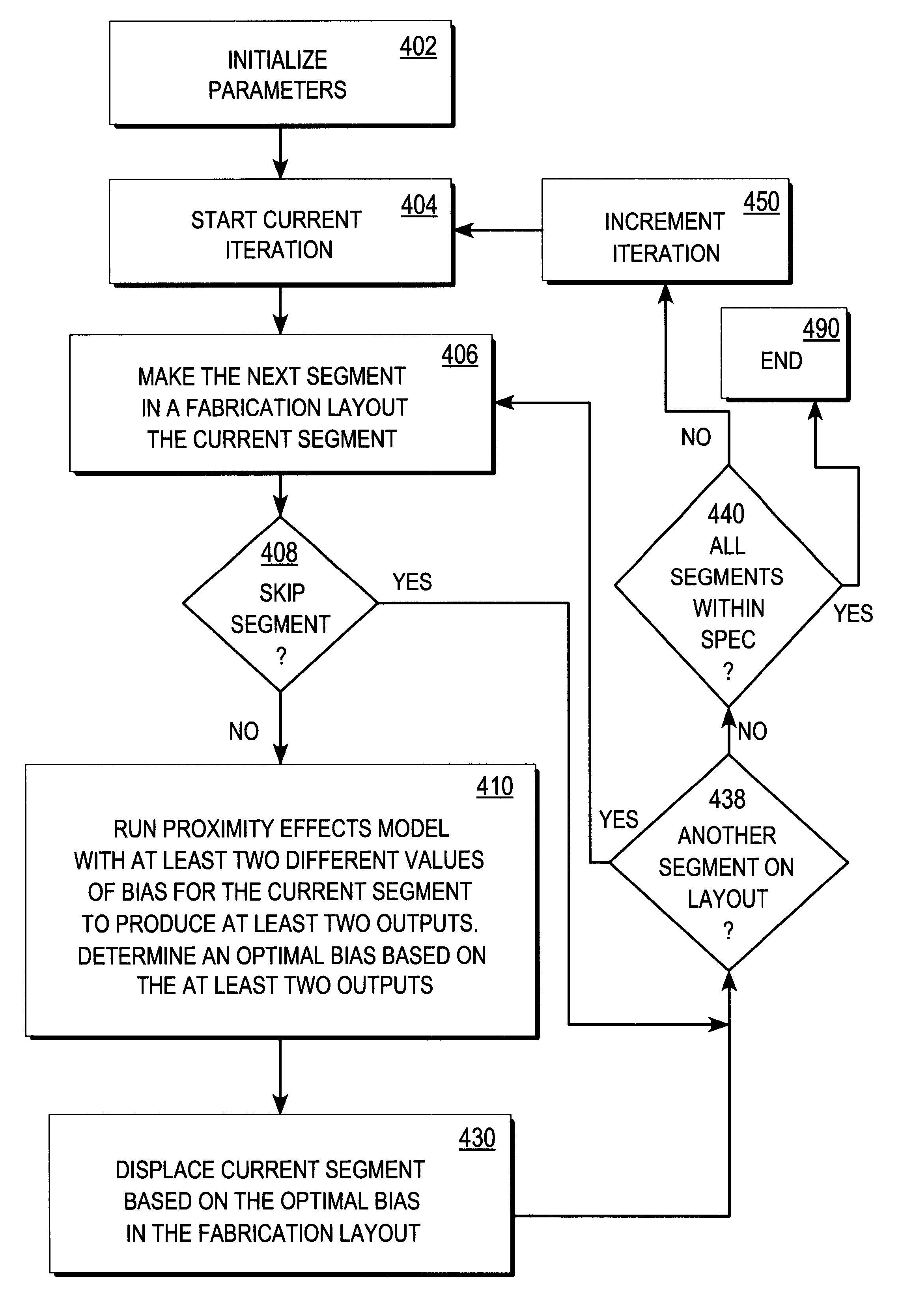
FIG. 7 is a flow diagram showing an iterative adjustment of a fabrication layout using an inverse proximity effects model, according to one embodiment of adjustment process 263 from FIG. 2.

In step 702, parameters used by the techniques are initialized. In step 704, the current iteration begins. A segment of the fabrication layout is visited only once per iteration. In step 706, one of the segments not yet visited in this iteration is made the current segment. In step 708, it is determined whether the current segment should be skipped. If the current segment is skipped, control passes to step 738 to determine whether another segment remains to be visited in the layout. If the current segment is not skipped, control passes to step 710 in which the inverse proximity effects model is run for the current segment. The inverse proximity effects model is run using the edges in the design layer as input. Then the output amplitudes indicating edges for the ...


PUM

PropertyMeasurementUnit
interior anglesaaaaaaaaaa
distanceaaaaaaaaaa
distanceaaaaaaaaaa

Abstract

Techniques for forming a fabrication layout, such as a mask, for a physical design layout, such as a layout for an integrated circuit, include correcting the fabrication layout for proximity effects using a proximity effects model. A proximity effects model is executed to produce an initial output. The initial output is based on a first position for a segment in a fabrication layout. The first position is displaced from a corresponding original edge in the original fabrication layout by a distance equal to an initial bias. The model is also executed to produce a second output based on a second position for the segment. The second position is displaced from the corresponding original edge by a distance equal to a second bias. An optimal bias for the segment is determined based on the initial output and the second output. The segment is displaced in the fabrication layout from the corresponding edge based on the optimal bias.

Description

1. The Field of the InventionThis invention relates to the field of printed feature manufacturing, such as integrated circuit manufacturing. In particular, this invention relates to computing corrections using a proximity effects model at evaluation points to achieve improved agreement between a design layout and an actual printed feature.2. Description of Related ArtTo fabricate an integrated circuit (IC), engineers first use a logical electronic design automation (EDA) tool, also called a functional EDA tool, to create a schematic design, such as a schematic circuit design consisting of symbols representing individual devices coupled together to perform a certain function or set of functions. Such tools are available from CADENCE DESIGN SYSTEMS and from SYNOPSYS. The schematic design must be translated into a representation of the actual physical arrangement of materials upon completion, called a design layout. The design layout uses a physical EDA tool, such as those available fr...

Claims


Application Information

Patent Timeline
Patent Type & Authority Patents(United States)
IPC IPC(8): G03F1/14G03F1/00G03F1/36G03F7/20
CPCG03F1/144G03F7/70441G03F1/36G03F1/68
Inventor PIERRAT, CHRISTOPHEZHANG, YOUPING
Owner SYNOPSYS INC
Why Eureka
Try Eureka