
Single-block virtual frame buffer translated to multiple physical blocks for multi-block display refresh generator

a multi-block display and virtual frame technology, applied in the field of frame buffers, can solve the problems of reducing the manufacturing yield, reducing the size of the soc die, and even becoming too expensive for many low-cost consumer devices

Inactive Publication Date: 2004-01-20
MIND FUSION LLC +1
View PDF9 Cites 42 Cited by
  • Summary
  • Abstract
  • Description
  • Claims
  • Application Information

AI Technical Summary

Problems solved by technology

However, larger, more colorful displays running at higher-resolution modes may require a large frame buffer to store a large number of pixels.
However, larger on-chip SRAMs increase the SOC die size and reduce manufacturing yield.
The SOC may even become too expensive for many low-cost consumer devices.
Re-writing the many programs that can run on the CPU to allow for a split frame buffer is not practical.
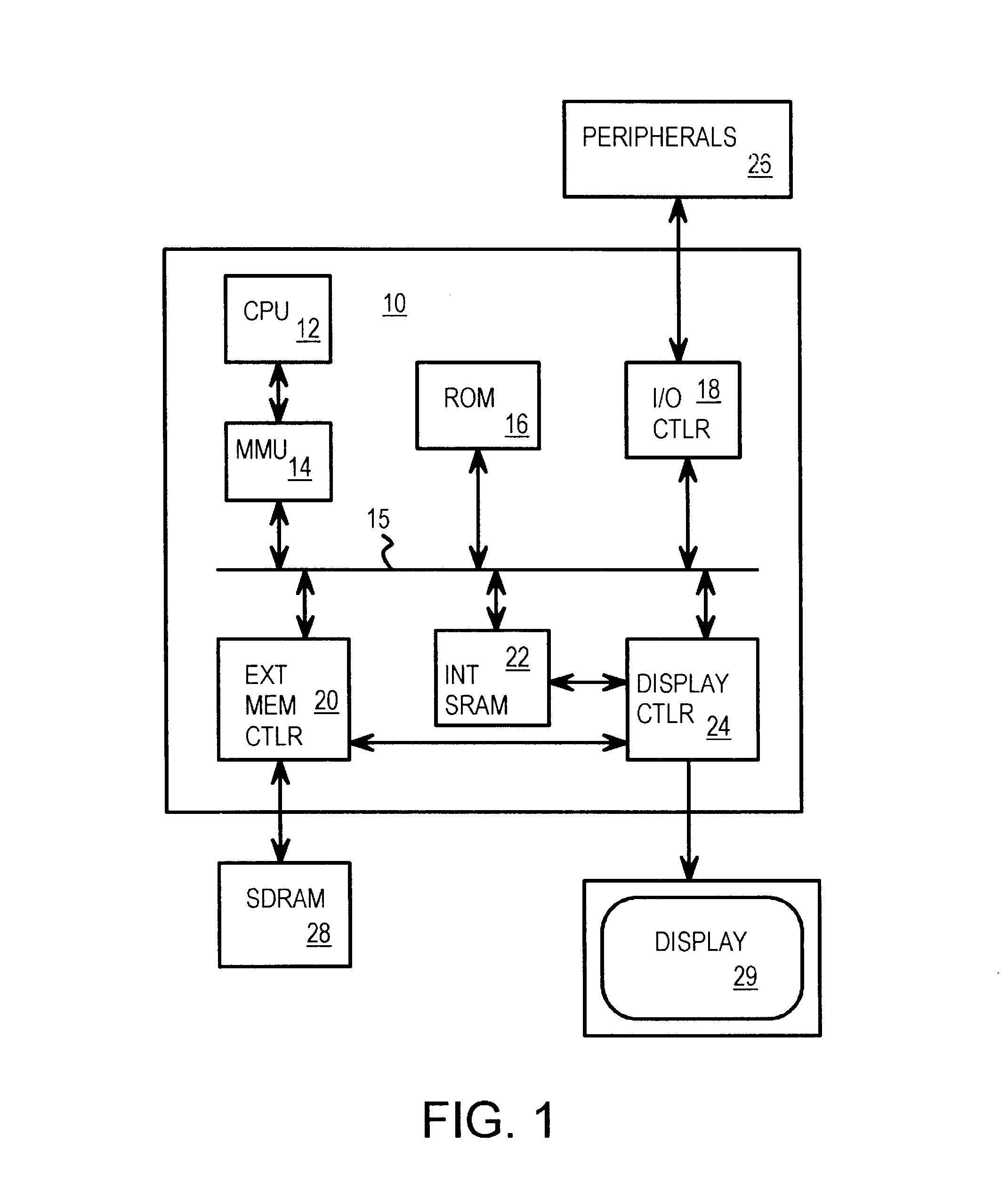
However, for higher-resolution, higher-color, higher-power display modes the frame buffer does not completely fit in SRAM 22.
Also, the access time may be slower for the external SDRAM than for the internal SRAM.

Method used


Image

  • Single-block virtual frame buffer translated to multiple physical blocks for multi-block display refresh generator
  • Single-block virtual frame buffer translated to multiple physical blocks for multi-block display refresh generator
  • Single-block virtual frame buffer translated to multiple physical blocks for multi-block display refresh generator

Examples


Embodiment Construction

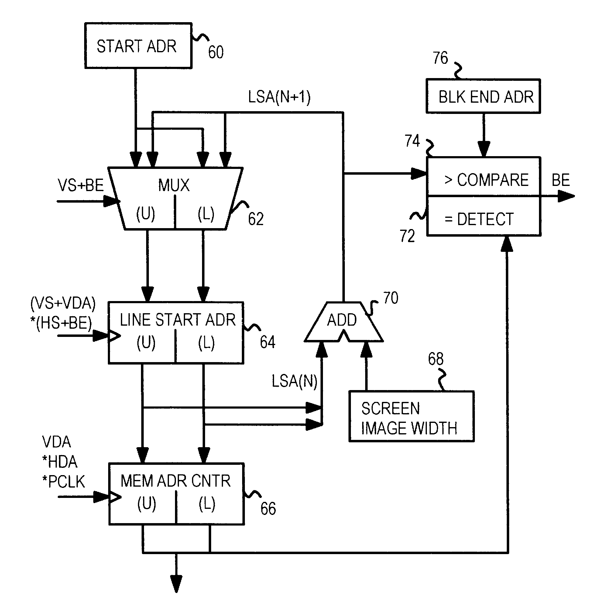
Several other embodiments are contemplated by the inventors. For example the address generator of FIG. 5 could be implemented in logic gates and registers, or programmably implemented, or some combination of dedicated hardware and firmware. Other kinds of address translation could be substituted, or paging could be implemented in a variety of ways.

The entire page (all offset address locations within a page) does not have to be used by displayable pixels. Some overhead storage locations may be located on the page, and the last page on a frame can have only some of the available space used. A typical system has many more pages than shown in the drawings. For example, a frame buffer that stores 1 M-byte of pixels uses about 256 physical pages when each page is 4K in length.

The physical address of the memory may be specified in units other than bytes. For example, the physical memory may be read in words of 4 or 8 bytes. The memory address counter can be made to increment by one memory ...


PUM


Abstract

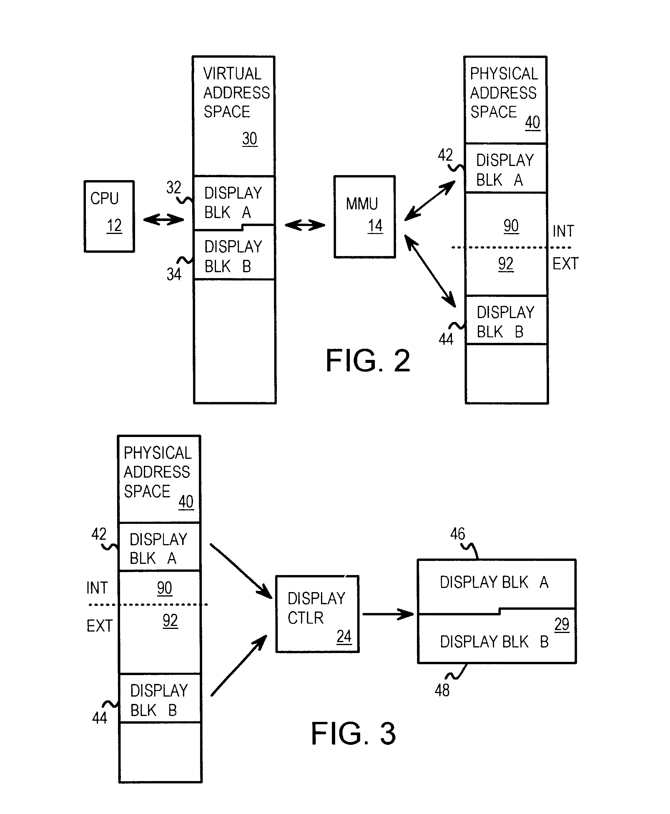
A graphics controller for a System-On-a-Chip (SOC) used with a battery-powered device allows for reduced-power display modes. The microprocessor writes to a frame buffer that is a single, contiguous address block in virtual memory. A memory management unit (MMU) translates frame-buffer address to multiple physical blocks. The graphics controller fetches pixels from the multiple physical blocks, including a block in an on-chip memory and a block in an external memory. In a low-power mode, pixels are only fetched from the lower-power on-chip memory and not the higher-power external memory. A smaller display window is defined and pixels outside the window are replaced by dummy data,.eliminating external-memory fetches. The smaller display window falls within the first block in the on-chip memory. Status and other information can be displayed in the smaller display window during stand-by modes, while a full-screen of data is displayed for full-power modes.

Description

BACKGROUND OF INVENTIONThis invention relates to computer-graphics systems, and more particularly to frame buffers split among multiple blocks in memory.An interesting variety of small consumer devices are appearing. Portable computing and / or communication devices such as the personal digital assistant (PDA), Pocket PC, and smart cellular phones have an astonishing computing power for such small devices. These portable, often hand-held, computing devices often use a very-large-scale-integration (VLSI) chip that includes a microprocessor or central processing unit (CPU), memory, and I / O controllers on a single silicon chip known as a System-On-a-Chip (SOC).These consumer devices run on battery power to achieve portability. The battery must be made small and light to keep the size and weight of the overall device small. Such small batteries necessitate the use of low-power chips including the SOC.The SOC can include an on-chip static random-access memory (SRAM). Program running on the...

Claims


Application Information

Patent Timeline
Patent Type & Authority Patents(United States)
IPC IPC(8): G09G5/39G09G5/36
CPCG09G5/39G09G5/14G09G5/363G09G5/393G09G5/395G09G2330/021
Inventor ISHII, TAKATOSHICHEUNG, EDMUNDBRANNON, SHERWOOD
Owner MIND FUSION LLC
Learn More