Display device

a technology of display device and display screen, which is applied in the field of display device, can solve the problems that display device also suffer from image retention, and achieve the effect of avoiding short circui

Inactive Publication Date: 2004-02-17
KONINKLIJKE PHILIPS ELECTRONICS NV
View PDF5 Cites 15 Cited by
  • Summary
  • Abstract
  • Description
  • Claims
  • Application Information

AI Technical Summary

Benefits of technology

Another object of the invention is to provide a display device in which the flicker problem is substantially reduced or eliminated.
Various amounts of the passivating material may be used, with preferred amounts ranging from about 1 nm to about 5 nm. It is important that the passivating material be present in amounts that result in thin films, so that when applied, it does not cause a short circuit among the many separate pixels of the display. We have found that when Au is the passivating material present in amounts that give rise to thicknesses from about 1 nm to 5 nm, the thickness of Au present cannot form a continuous film bridging otherwise separate Al metal regions, due to the thickness of the Al, and the resulting surface texture. Thus, it is possible to take advantage of the step coverage to avoid shorting out the circuit.

Problems solved by technology

The display devices also often suffer from image retention.

Method used


Image

  • Display device
  • Display device
  • Display device

Examples


Embodiment Construction

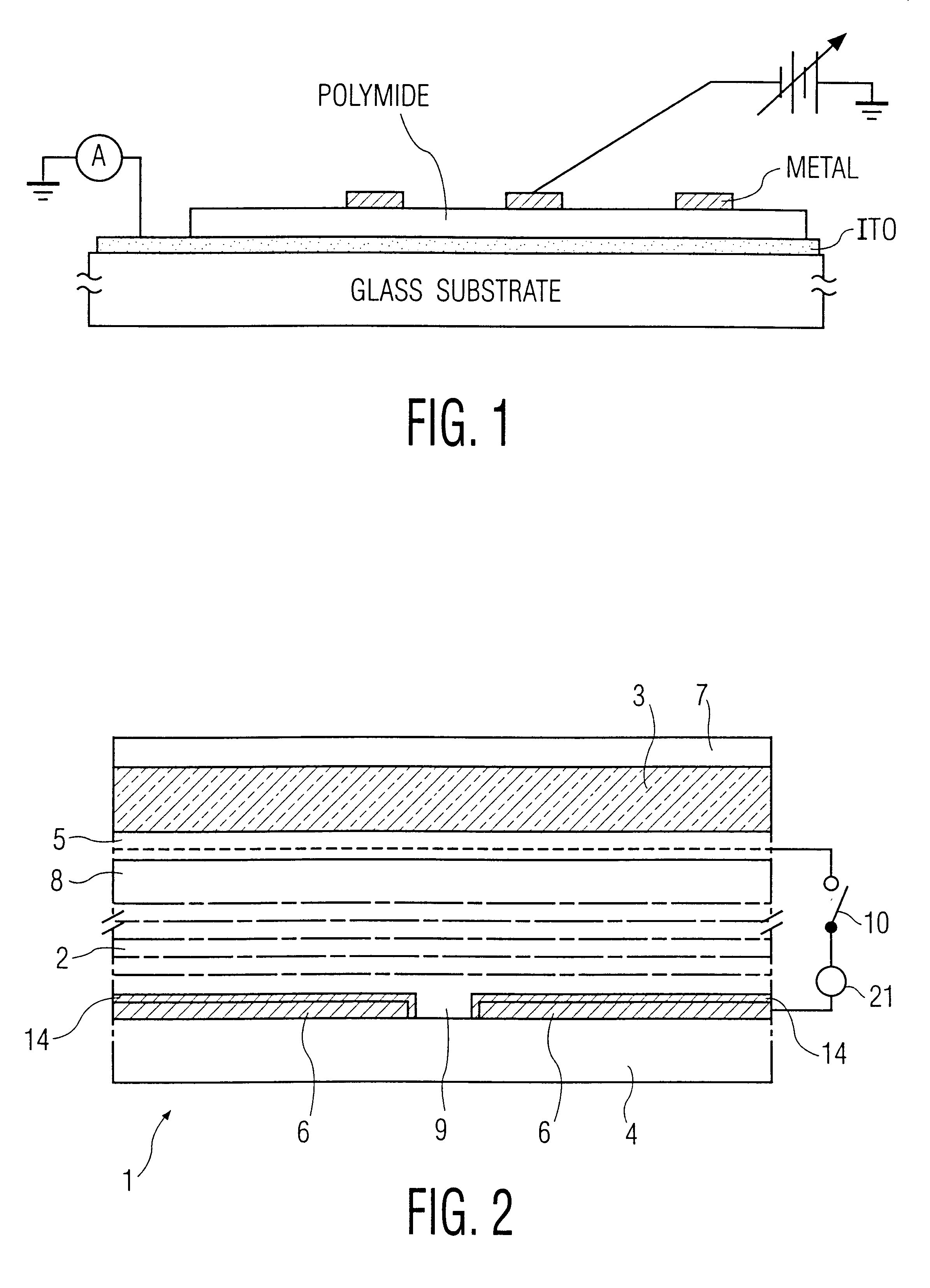
With reference to FIG. 1, there is illustrated a test structure, which comprises only some of the parts of a LC cell, and which was devised to test the effectiveness of the use of a passivating material in a display device. A glass substrate with an ITO layer was spin-coated with polyimide. A small region of the ITO layer was left uncoated to serve as the back electrode contact. This structure was then placed on a shadow mask, and circular dots of metal were evaporated onto the polyimide surface. Various metals were tried including Au, Al, Ti, and combinations thereof. All other parameters of the test structures were identical. FIG. 1 is also a schematic cross-section, including a schematic of the electrical connections for I-V measurements. The test structures were measured electrically. dc I-V measurements were made for applied voltages in the range of -0.5 to +0.5 V. This arbitrary value was chosen as representative of the field across the polyimide under typical reflective-LCD o...


PUM

PropertyMeasurementUnit
thicknessaaaaaaaaaa
thicknessaaaaaaaaaa
flicker frequencyaaaaaaaaaa

Abstract

A display device is provided which includes a first substrate having at least one transparent, first picture electrode of a first material, a second substrate having at least one second picture electrode of a second material which, jointly with the picture electrode on the first substrate and an intermediate opto-electronic material, defines a pixel, and means for supplying electric voltages to the picture electrodes, wherein at least one of the picture electrodes is coated with at least one layer of a passivating material such that any asymmetry in operation of the device is substantially reduced or eliminated.

Description

FIELD OF THE INVENTIONThis invention relates to a display device comprising a first substrate having at least one transparent, first picture electrode of a first material, a second substrate having at least one second picture electrode of a second material which, jointly with the picture electrode on the first substrate and an intermediate opto-electronic material, defines a pixel, and means for supplying electric voltages to the picture electrodes.BACKGROUND OF THE INVENTIONDisplay devices of this type are generally known and usually comprise a large number of pixels. The first type comprises, for example, LCDs, both of the passive and active type; the second type comprises, for example, plasma-addressed liquid crystal display devices referred to as PALC displays.Notably when the second picture electrode is reflective, the drive of these display devices appears to be sensitive to the alternating supply of positive and negative voltages across the pixels. This becomes manifest as, f...

Claims


Application Information

Patent Timeline
Patent Type & Authority Patents(United States)
IPC IPC(8): G02F1/13G02F1/1335G02F1/1343G02F1/1362G02F1/136G09F9/30
CPCG02F1/133553G02F1/13439G02F1/136277
Inventor MARSHALL, THOMASHABERERN, KEVIN W.
Owner KONINKLIJKE PHILIPS ELECTRONICS NV
Why Eureka
Try Eureka